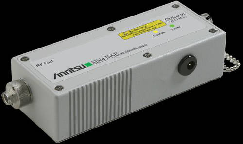
Thanks to these options, the MN4765B can be used with the MS4640B VectorStar® family of vector network analyzers to perform optoelectronic measurements up to 70 GHz for wavelengths of 1310 nm and 1550 nm.
Option 71 allows the MN4765B to be used with the VectorStar vector network analyzer to perform optoelectronic measurements between 70 kHz and 70 GHz within the 1310 nm range, while Option 72 provides measurements between 70 kHz and 70 GHz for 1310 nm and 1550 nm. Both options employ a NIST-characterized photodiode as the primary standard to achieve superior electro-optical and optoelectronic measurement accuracy compared to alternative methods.
The MN4765B module, when paired with the MS4640B vector network analyzer, provides a simplified solution for optoelectronic measurements and offers a cost-effective alternative to conventional complete system solutions currently in use. The MN4765B optical modules are designed with an InGaAs photodiode that converts modulated optical signals into electrical signals. The photodiode boasts an exceptional bandwidth response up to 70 GHz. The modules also incorporate additional circuitry for temperature and polarization stability.
With the new wavelength options, the MN4765B optoelectronic calibration modules can be used to perform two-wavelength optoelectronic measurements to characterize components in R&D and manufacturing. They are also suitable for universities and research laboratories studying modulation rates up to 70 GHz at two wavelengths.
VectorStar vector network analyzers provide more accurate measurements across single-sweep frequency ranges from 70 kHz to 20 GHz, 40 GHz, 50 GHz, 70 GHz, 110 GHz, 145 GHz, and various discrete bands up to 1.1 THz. Unlike other vector network analyzers on the market, the VectorStar family is built on a stable, modern platform that can be easily adapted to various functions and performance requirements. The MS4640B series of vector network analyzers offers a high level of performance, enabling device modeling engineers to accurately and reliably characterize their devices. R&D engineers can extract every last fraction of a dB from their most advanced designs, and manufacturing engineers can maximize throughput without sacrificing accuracy.