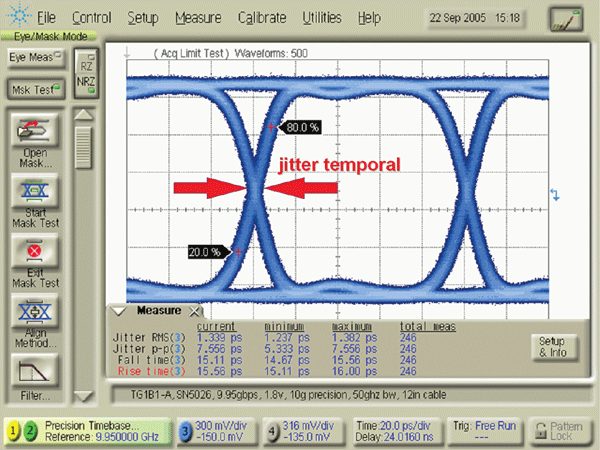
 Throughout a digital communications system, data signals are subject to numerous sources of noise and unwanted effects that degrade their quality. One such degradation is jitter (Figure 1), which manifests as temporary fluctuations in the bit periods of the digital signal, hindering the sampling and recovery of data at the receiving end. Depending on its bit rate, the data signal will be more or less affected by jitter. However, in all cases, there are maximum jitter levels that must be ensured. The International Telecommunication Union, in its ITU-T Recommendation G.783, specifies the jitter requirements for SONET/SDH digital optical signals. The jitter limit values are summarized in Table I. As can be seen, in all cases, a maximum jitter of 10% of the bit period is assumed, although the measured values depend on the frequency range considered and, above all, on the bit rate of the digital signal. At high speeds (10 and 40 Gbit/s), jitter measurements must be quite precise. Therefore, high-performance instrumentation, such as that presented in this article, is required.
Sources of Jitter. Jitter in optical communication networks can originate from various sources. To describe the influence of each, it is helpful to analyze the system's block diagram. The most basic block diagram consists of an optical transmitter, an optical receiver, a fiber optic link, and a reference clock (Figure 2). The reference clock determines the system's bit rate. If the clock frequency fluctuates over time, the bit rate will also fluctuate, and the data signal will experience jitter. The mechanisms causing jitter in the reference clock can be varied: random jitter due to oscillator noise, periodic jitter due to spurious sidebands, or duty cycle distortion due to oscillator nonlinearities.
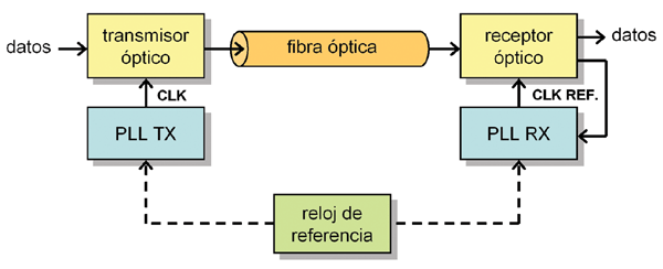 To generate the data signal, the transmitter receives the reference clock as an input signal. Typically, this reference clock is used as the base frequency from which the bit rate to be transmitted is generated. The process of multiplying this reference frequency is performed using a PLL, which also contributes to jitter. In this case, it's random jitter originating from its internal oscillator (VCO, voltage-controlled oscillator). The input jitter (from the reference clock) is filtered by the PLL's transfer function. Since this is a low-pass filter, the high-frequency components of the jitter are eliminated. However, the low-frequency jitter remains. On the other hand, the VCO jitter is affected by a complementary transfer function, as the VCO is located within the PLL loop. Therefore, in this case, the low-frequency components of the VCO jitter are eliminated, while the high-frequency components remain. Additionally, noise from other elements in the loop, such as amplifiers or a phase detector, can be added to the VCO jitter, resulting in a more complex jitter spectrum. The main conclusion is that the PLL bandwidth has a significant influence on data signal jitter levels, and frequency-domain jitter spectrum analysis provides valuable information about how jitter propagates and how to control it.
 While these jitter sources are primarily electronic, optical components also contribute to increased jitter levels. For example, the laser transmitter and optical amplifiers generate RIN and ASE noise, respectively, which degrade data signal quality. Even phase noise (linewidth) or chirp from the optical transmitter is problematic, as its combination with chromatic dispersion in the fiber (PM-IM conversion) generates intensity noise and jitter. In short, optical fiber as a transmission medium is not immune to introducing jitter. At high speeds (e.g., 40 Gbit/s), polarization dispersion (PMD) is also a frequent cause of degradation, limiting the range of dispersion-compensated fiber links to a few kilometers.
The receiver in the communication system then has to handle a degraded signal and recover the data with minimal errors. The receiver itself can also contribute to jitter through mechanisms similar to those in the transmitter circuitry. Since jitter directly affects the bit error rate (BER), there is a maximum jitter value (for each bit rate) that allows the system to function correctly. If this value is exceeded, some form of 3R regeneration will be necessary to reduce jitter levels.
Jitter Measurements
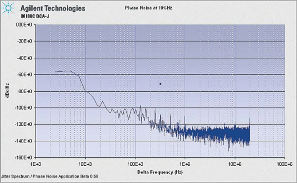
To verify if the system is within the jitter specifications (Table I), measurements with high-performance instrumentation are required. It is generally very useful to examine the spectral broadening of the signal. The broadening of the clock signal spectrum is usually symmetrical, so analyzing the spectrum of the upper modulation band with respect to the center frequency of the ideal carrier (offset) is sufficient. Since this broadening is normally due to random noise processes, the energy is measured by averaging over 1 Hz intervals. This yields a phase noise graph like the one shown in Figure 3. The units are dBc/Hz, as the measurement result is normalized with respect to the total signal energy. This graph shows that random jitter is composed of different noise mechanisms, each with a distinct nature: frequency-independent phase white noise, phase modulation flicker noise (dependence as 1/f), FM white noise (dependence as 1/f²), FM flicker noise (dependence as 1/f³), and random-path FM noise (dependence as 1/f⁴). This method of jitter analysis is preferred by wireless system designers and can be measured using a spectrum analyzer. However, for optical communication links, it is preferable to represent the jitter spectrum in RMS seconds, as this provides more information when comparing signals with different bit rates. In this case, it is impossible to obtain jitter measurements by analyzing phase noise on a spectrum analyzer, so other types of instrumentation must be used. Equipment from multiple manufacturers is available on the market for measuring jitter in digital optical systems. These are not specialized devices, but rather oscilloscopes and digital signal analyzers that serve multiple purposes, including the ability to accurately determine the jitter of input optical and/or electronic signals. Figure 4 shows some of the 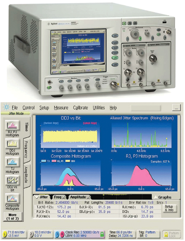 typical measurement results that can be obtained with one of these devices. Specifically, it is the Agilent Digital Communications Analyzer (Infiniium 86100C DCA-J). As can be seen, the device allows for obtaining the total jitter (TJ) value, as well as separating the different contributions: data-dependent jitter (DDJ), including intersymbol interference (ISI) and duty cycle distortion (DCD), periodic jitter (PJ), and random jitter (RJ). Additionally, Figure 4 displays various histograms of the measured jitter values. These allow for observing the dispersion of the jitter values, as well as calculating the RMS values.
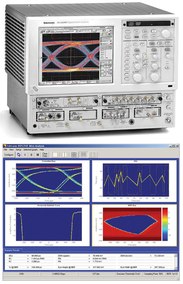
Other equipment available on the market includes the Anritsu MP1800 signal analyzer and the Tektronix DSA8200 digital sampling oscilloscope. For the MP1800 (Figure 5), several options have recently become available that allow for jitter measurements on signals up to 50 Gbit/s. Specifically, these include the 12.5 GHz 4-port synthesizer (MU181000B), jitter modulation options (MU181000A/B-001), and the jitter measurement software application (MX180005A). The Tektronix DSA8200, on the other hand, also allows for the analysis of 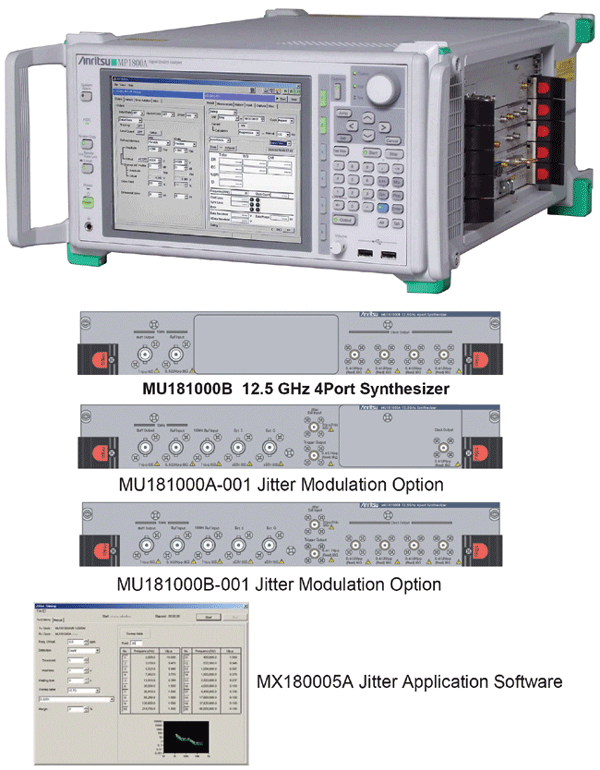 jitter in digital optical signals up to 43 Gbit/s using the 80SJNB software application. Additionally, the team identifies and isolates the causes that affect the horizontal and vertical opening of the eye diagram, separating the effects of jitter and noise.
Francisco Ramos Pascual. PhD in Telecommunications Engineering.
Full Professor at the Polytechnic University of Valencia.