 In this article, we will examine the performance variations of modern, high-density connection models. The models will be derived from both simulation and measurements and then compared. Real-world variations due to the effects of incomplete inserts and soldering will be considered. Finally, model quality metrics will be applied to the data to quantify the accuracy of the models.
 Evolution of connector models.
Connector models have evolved from simple lumped-parameter coupling circuits to multi-port microwave networks. This increased complexity is driven by the need to accurately represent bandwidths with increasingly complex geometric discontinuities.
Early connector models were simply lumped-parameter circuits. These models are very simple, run quickly with simulation software, and are still in use today for many applications.
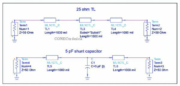
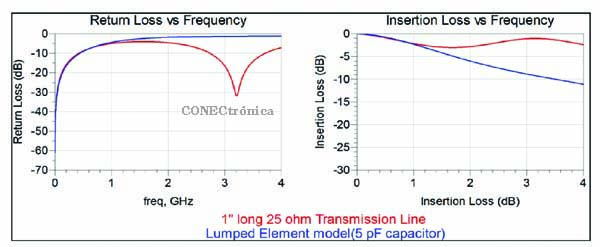
The generally accepted gold standard is that a representation of a piece of transmission line elements is valid as long as the length of the transmission line (L) is less than one tenth of the wavelength (L
Using L's golden rule.
The logical extension of a lumped-parameter circuit is a distributed-parameter model.
The transmission line is divided into several smaller sections, and the bandwidth model can be easily expanded.
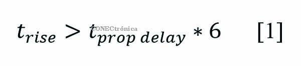
This relationship can be expressed in the time domain by the following equation:
This equation states that a lumped-parameter circuit method is valid as long as the connector propagation delay (tprop delay) is greater than 6 times the system rise time (trise). A 10 mm stackable connector has a propagation delay of approximately 60 ps, so a simple lumped-parameter circuit is a reasonable model as long as the system rise time is 360 ps.
This was the case for many digital applications in the 1990s. Of course, this simple connector model does not include the effects of interference.
The complexity of the model increases with increasing timing frequencies and rise times. The lumped parameter circuits became more refined as the connector was broken into several shorter sections.
Each section was analyzed using 2D finite element analysis (FEA) codes to obtain an inductance (L) and capacitance (C) matrix with coupling terms (K) for the transmission line coupling. The K values account for interference in multi-conductor transmission lines.
These L, C, and K values could be translated into SPICE models and accurately predicted interference, propagation delay, and impedance.
 The 2D analysis of multiple cross-sections of connectors was not a simple process.
Engineering judgment was needed to select the fewest possible cross-sections while achieving a high degree of accuracy. The 2D modeling approach assumed TEM propagation throughout the connector structure. Because this was not actually the case, evanescent waves at internal discontinuities were ignored, leading to inherent inaccuracies in the process. Nevertheless, the multiple cross-section method remained common practice into the late 1990s.
To overcome these limitations, software vendors began working diligently on creating tools that would improve service to the high-speed digital industry. Full-wave simulation was the standard for microwave (coaxial) connectors during this period. The geometric complexity of a modern high-speed digital connector presents a significant challenge, as it cannot be solved with affordable computing hardware. As the computing power of high-end workstations increased, high-speed digital connectors could be treated as multi-port microwave networks. This is the current state of connector modeling.
Connector Models from Simulation:
Several simulation tools are available to the signal integrity (SI) engineer to extract connector models. CST Microwave Studio was used in the course of this work. While a specific tool was used, the issues raised are common among all full-wave modeling tools.
To put the scope of the modeling challenge into perspective, geometry must be considered. A typical high-density connector might have 10 rows with 50 pins per row in a 1.27 mm x 1.27 mm pitch. This density is driven by the need for high-density electronic packaging and limited by stamping, casting, and assembly technologies.
Figure 3 shows a typical mezzanine connector that will be referenced in this article.
This type of connector has an open-path field, meaning there are specific pins not dedicated to the current return (ground). A signal-to-ground pattern is defined for a given application that provides the highest signal density with acceptable signal performance. Predefined patterns for differential and single-terminal signaling are developed, and modeling software is used to extract a Touchstone model.
Fortunately, not all 500 pins need to be included in the extracted model, but the magnitude of the problem is significant. A reasonably sized model might include six differential pairs to capture the effects of interference within and between rows. This would be equivalent to a 24-port Touchstone model.
For a right-angle version of a similar connector, a larger port model is typically considered to account for the varying lengths of each row. Recognizing this for each modeled differential pair, the signal return pins are also included in the modeling area, so this 24-port Touchstone model will include 12 signal pins and 8 ground pins. Each pin has a complex shape to provide the normal force to the detachable interface necessary for a reliable connection.


SolidWorks, the 3D CAD package, is a tool that can be used to design the connector. The geometry is exported to a format that can be read by the full-wave simulation tool. Then, "geometric cleanup" is performed—a critical phase in modeling where unnecessary complexity is removed. This results in a cleaner import process in the full-wave simulation tool and simplifies the mesh. This area of geometry input has been problematic and has been the focus of considerable investment by full-wave simulation tool vendors.
Once the geometry is imported correctly, there are three main steps that must be performed before starting the simulation:
1. Mesh density
2. Definition of material properties
3. Port configuration.
Mesh Density:
All full-wave simulation tools perform electromagnetic computations on a discrete solution space. The discretization, or meshing, process divides the solution space into many cells and has a direct impact on the resulting solution. A mesh that is too fine leads to erroneous results, and a mesh that is too fine leads to unnecessarily long simulation times. Finally, mesh density and simulation time are affected by the maximum simulation frequency. A 50 GHz simulation will be meshed much more finely than a 20 GHz simulation.
CST Microwave Studio will create a mesh of the solution space using very basic information to simplify a complex process. The maximum frequency and the number of cells per wavelength in the x, y, and z directions are all that is needed. After automatic meshing, mesh refinement is possible in regions of high field concentration. For example, a microstrip substrate mesh is often refined by the user if high return loss accuracy is required.
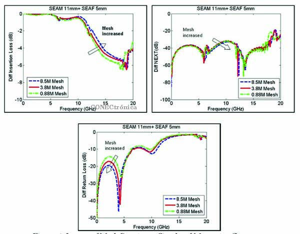
To investigate the impact of the meshing process on typical connection models, a 16 mm mezzanine connector was simulated and the mesh parameters were adjusted in the CST
Mesh sizes: 0.88 million cells, 3.8 million cells, and 8.5 million cells. The variation with mesh density is smaller in this example, with return loss being the parameter most sensitive to meshing.
Material Parameters:
Many high-speed connectors are designed using liquid crystal polymers (LCPs) as the connector encapsulation. LCPs are an anisotropic, homogeneous dielectric whose mechanical properties vary depending on the molding process. It is assumed that the electrical properties also vary with the molding, but little research has been published to date on this effect.
LCP manufacturers provide dielectric constant values based on standardized tests of 3-inch circular disks.
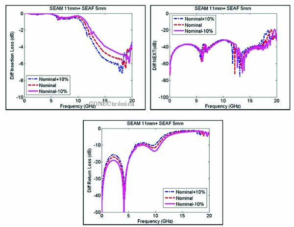
To investigate the impact of dielectric constant variation on typical connection models, simulations were performed over a range of dielectric values. The results for three different LCP dielectric constants are shown in Figure 5. As with mesh density variation, return loss is affected by the LCP dielectric constant. Insertion loss (IL) above 10 GHz is also affected. This is consistent with the change in reflection loss due to impedance mismatch seen in the return loss profile in Figure 5. For the mezzanine connector in this report, a first-order constant Debye model was used in CST Microwave Studio.
Port Configuration
The third most important step in extracting a connector model using a full-wave simulation tool is port configuration.
A port defines how an electromagnetic structure is stimulated and from where the response is measured. There are usually several port options available in modern full-wave simulation tools, but they generally fall into two main categories: waveguide ports and discrete ports. A waveguide port projects a TEM or quasi-TEM wave onto the structure, typically a well-defined transmission interface such as a coaxial line or microstrip. The transmission line must generally be of a certain length for this method to be valid. A discrete port is a theoretical circuit approximation commonly used in very dense structures where a waveguide port is not feasible due to its size.
The port configuration also defines the location of the reference plane for the resulting connector model.
The connectors of interest in this article are soldered onto a multi-layer PCB, and PCB effects are generally included in the connector model. The location of the reference plane determines the extent of PCB effects included in the model. For the mezzanine connector in this report, a discrete port was used in CST Microwave Studio.

Connector Models from Measurement:
To have confidence in a connector model, it is good engineering practice to validate the model. Validation can be done by comparing the model to one extracted using a different method, either through measurements or by comparison with other modeling tools. While comparing models extracted using different tools is widely accepted in some industries, the high-speed digital community generally prefers model validation through measurements. There are pitfalls to this approach, as measured results can vary widely depending on the test fixtures, the location of the reference plane, and calibration. The high-density connectors that are the subject of this article do not have coaxial interfaces that mate with modern instrumentation. Instead, a test fixture is required to interface with the instrumentation leading to the device. This is typically a multilayer PCB that includes the effects of the connector's size. The effects of pad capacitance and via stud are considered size effects. It is generally accepted that these size effects between the PCB and the connector are included in the connector model.
For model correlation, the test device needs to be included in the simulation or removed from the measurement using de-embedding techniques. Due to the model's complexities, de-embedding the test device is preferred. The de-embedding method will utilize the TRL/M (Thru-Reflect-Line-Match) method available on a modern vector network analyzer (VNA).
The accuracy and validity of any VNA measurement depends on the extent to which implicit calibration assumptions are violated. For example, a SOLT (Short-Open-Load-Thru) calibration is compromised by poorly developed calibration standards.
If the open calibration standard has parasitic capacitance, this must be taken into account in the calibration process, as it violates the assumption that the aperture has a unit reflection coefficient. This is why instrumentation manufacturers develop highly accurate SOLT calibration standards.
Removing the fixture using TRL/M calibration is no different; poorly developed calibration standards will result in measurement inaccuracies.
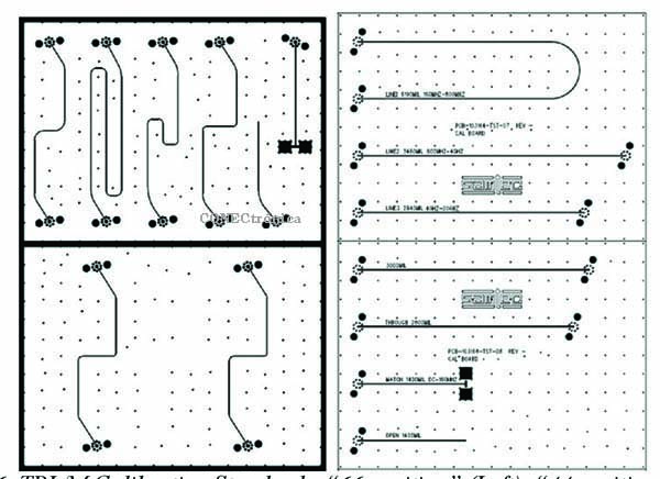
One assumption of the TRL/M method is that line standards have the same impedance as the fixture. This seems reasonable until we consider that the industry standard impedance control for high-density PCBs is +/-10%. To illustrate the impact of standard line impedance, we considered two different sets of onboard TRL/M calibration standards, as shown in Figure 6. Note that the calibration footprints on the PCB at position 66 have reasonable, but sharper, curves compared to the curves at position 44. These calibration footprints were tested for impedance, and the calibration footprints with sharper curves (position 66) were found to have more impedance variation than the calibration footprints with fewer curves (position 44). This impedance variation translates into measurement error with TRL/M calibration.
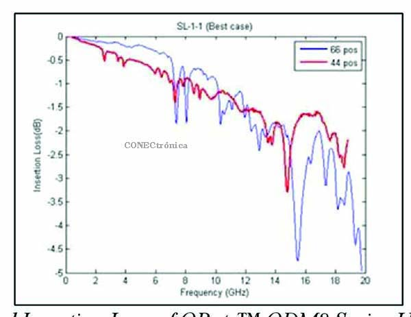
Figure 7 shows the variation in measured insertion loss of the same type of connector, using two different test devices with their associated onboard TRL/M calibration standards.
In principle, the two curves in figure 7 should be identical; instead, we see a variation of approximately 0.5 dB and some changes at some resonance points.
This example also illustrates a common problem with accessory design where small size differences can manifest as significant variations in connector measurement.
A detailed examination of the results reveals minor differences, as shown in Figure 8. Note that the trace of the pad grounding through the connector pad is slightly longer in the “position 66” case compared to the “position 44” case. This minor size difference resulted in the resonance change observed in Figure 7 and was verified through full-wave modeling of the connector and its size.
The previous example is a good case study, but in reality, there are two variables: size differences and standard TRL/M calibration variations.
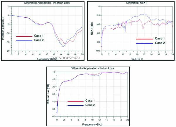
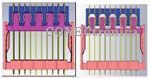
The following example has only a small size variation. Figure 9 shows two different sizes: Case 1 and Case 2.
Case 1 on the left has the ground paths "outboard," or away from the center of the connector. This method results in more optimal return current flow, but at the expense of a more complex routing pattern.
Case 2 on the right has the ground paths "inboard," or toward the center of the connector. Note that this routing results in more generous spacing between the signal traces and the ground path.
Figure 10 shows that there is a 10 dB variation in interference at 10 GHz due to this smaller variation in the ground path orientation.
Mechanical Variations:
There are mechanical variations involved in the test structures (and real-world products), including insertion depth and weld variations. Often, the SI effects due to these variations are overlooked, but frankly, they should be analyzed.
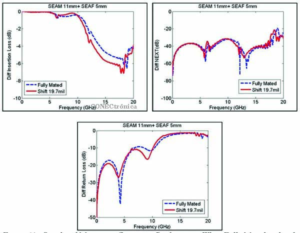
The first mechanical variation to consider is the connector's insertion depth. With any high-density, multi-pin connector, there is a built-in mechanical tolerance to accommodate the tolerance built into the mechanical package. Figure 11 illustrates the mechanical variation in a mezzanine connector. This product will maintain sufficient strength at the contact interface with up to 1.15 mm of separation. The connector was simulated when fully mated and at maximum separation using CST Microwave Studio. Care was taken to account for the variation in contact shape between the cases and to include the larger air gap when the two halves are separated. The results are shown in Figure 12 and exhibit approximately the same level of variation as was seen by varying the mesh density and changing the dielectric constant of the connector package.
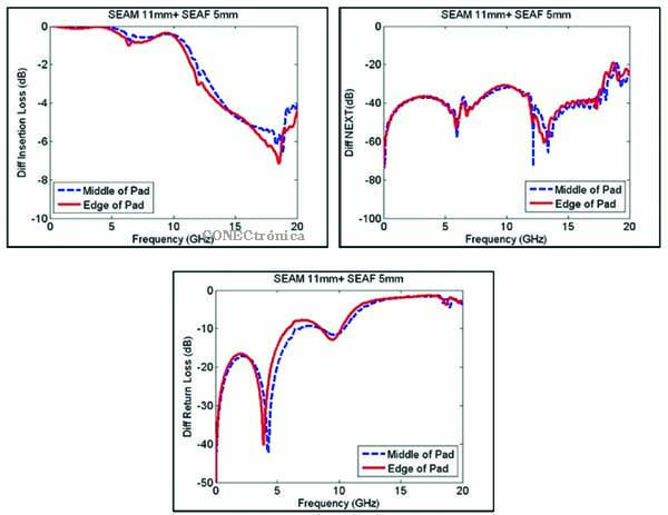
A second mechanical variation, which is assumed to be minor, is the variation in board mounting. For a surface-mount connector, the connector does not always sit flush against the
PCB's BGA pad. Tolerances in the PCB layout and mounting variation can cause some degree of fluctuation with the actual position.
Figure 13 illustrates this variation in positioning.
The results of these simulations for plate attachment are shown in Figure 14. Compared to changes in mesh density and dielectric constant variation, plate attachment has a relatively small effect.
The main takeaway from these examples is that measuring connector response can be as complex as extracting a connector model from a simulation. Care must be taken to ensure that the measured and modeled structures are exactly the same before attempting any correlation.
(To be continued in September)
Author:
Jim Nadolny, Samtec
Leon Wu, Samtec