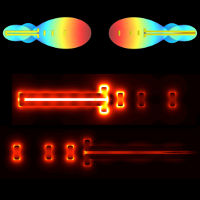
 Current prototypes of future nanochips use plasmonic or silicon waveguides for high-speed data transmission via light beams. The problem is that these waveguides result in significant energy losses and occupy a large amount of space. This space, along with the considerable heat dissipation, limits the integration and miniaturization capabilities of nanochips. The work developed here allows for the elimination of these waveguides, which would be replaced by a novel concept in optical communications: directional beamlinking with nanoantennas, or nanolink.
These types of links, after dominating radio frequency and microwave telecommunications for decades, are poised to revolutionize optical communications. The fundamental challenge for their application at these frequencies, aside from the technological difficulties involved in their fabrication, lies in the plasmonic electromagnetic behavior of nanomaterials when interacting with light. This behavior is very different and much more complex than that of the same materials at conventional frequencies. The Universities of Extremadura and Vigo have demonstrated that, by accurately calculating the plasmonic response using rigorous electromagnetic simulation tools and supercomputers, classical electromagnetic theory and the knowledge acquired over decades of development in the field of radio frequency and microwaves can be applied to the design of new nanotechnology applications.
The application used for this purpose, HEMCUVE++, has been continuously developed by the Universities of Extremadura and Vigo over more than 13 years. This tool has the fundamental quality of combining high calculation accuracy with the efficient use of large supercomputers. For this reason, in 2009 the Universities of Extremadura and Vigo were awarded two prestigious international prizes for their contribution to the introduction of supercomputing in electromagnetism. On this occasion, the Lusitania supercomputer at CénitS in Extremadura and the FinisTerrae supercomputer at CESGA were used for the design of the various components of the optical nanolink.
This work, recently published in an international journal, was funded by the Spanish National R&D Plan and the European Regional Development Fund (ERDF). It also received funding from the CONSOLIDER TERAENSE project and the Government of Extremadura. The original work is available at the following link: j.mp/nanolink