The proposed ROADM is compatible with both wavelength division multiplexing (WDM) and mode division multiplexing (MDM) systems. Unlike traditional ROADM devices for WDM-MDM systems, our innovation allows for the simultaneous reconfiguration of mode and wavelength dimensions through a single add/drop port. The insertion loss of the optical links, including mode coupling loss and crossover loss, is less than 7.0 dB, while the crosstalk of the manufactured device is kept below -13.4 dB. Furthermore, each individual add/drop port of the device can simultaneously offload multiple data signals onto a single bus waveform, paving the way for potential applications in future ultra-high-capacity data centers.
1. Introduction
Over the past decade, the rapid development of supercomputing, cloud services, and Internet of Things technology has propelled the field of on-chip optical information processing into a period of rapid growth. This growth is attributed to the superior advantages of optical information processing over traditional electronic information processing, such as higher bandwidth and processing speeds [1–4]. To meet the increasing performance demands of optical networks, various multiplexing technologies have been proposed and experimentally demonstrated to enhance data processing capabilities, including wavelength division multiplexing (WDM) [5–7], polarization division multiplexing (PDM) [8–10], and mode division multiplexing (MDM) [11–14]. Among these, MDM technology has garnered significant interest because it allows for improved optical link capacity using a single laser source. Currently, a high-order mode (de)multiplexer with 16 mode channels has been demonstrated [15], implying that the processing capacity of the devices can be increased up to 16 times that of a single-mode channel. Furthermore, by integrating MDM technology with WDM technology, the number of data channels in bus waveguides can be significantly increased. Numerous on-chip optical devices adapted to WDM-MDM systems have been proposed, such as the wavelength mode (de)multiplexer [16,17], mode-switching devices [18,19], and transmitters [20,21]. As WDM-MDM systems continue to evolve and expand, researchers have developed a variety of devices for processing information within WDM-MDM optical networks. Among these devices, the reconfigurable optical add/delete multiplexer (ROADM) stands out for its ability to load and unload data on bus waveguides, which plays a crucial role in the operation of WDM-MDM systems.
Several ROADMs have been proposed and demonstrated for MDM and WDM-MDM systems [22-25]. For example, one type of ROADM has been proposed that achieves effective selective access to any mode/wavelength channel by redistributing the mode field. This ROADM is capable of reconfiguring wavelengths at a single add/delete port by controlling the resonant wavelength of the microring switches [26]. However, for WDM-MDM systems, none of the previously proposed ROADMs have been able to achieve reconfigurability in both the wavelength and mode dimensions at a single add/delete port. As the number of channels increases, the number of add/delete ports in the ROADMs increases inappropriately, resulting in a more complex optical network. Therefore, achieving reconfigurability in both the wavelength and mode dimensions at a single upload/download port is essential.
In this work, we propose a ROADM for WDM-MDM systems based on the silicon-on-insulator (SOI) platform, which exhibits excellent reconfigurability in both wavelength and mode dimensions within a single add/delete port. Furthermore, the proposed ROADM effectively addresses the limitation that only one channel can be transmitted or received simultaneously on an add or delete port. As a proof of concept, we demonstrate a ROADM incorporating nine data channels (three wavelength channels and three mode channels) within a bus waveguide. By controlling the switching matrix, local data can be simultaneously loaded onto three channels through a single add port, while the download port can download the corresponding three channels. The insertion loss (IL) of the optical link is less than 7.0 dB and comprises primarily mode coupling and crossover losses. Additionally, the crosstalk (CT) of the fabricated device is better than -13.4 dB. The proposed device offers excellent scalability and reconfigurability, allowing each add/delete channel to simultaneously download and upload multiple signals, thus meeting future demands for higher data capacity.
2. Device Principle and Fabrication
Figure 1(a) shows the schematic diagram of the proposed ROADM, which contains two mode (de)multiplexers (M-(DE)MUX) and an n×n switching matrix based on micro-ring resonators (MRR). All components and waveguides are designed for quasi-transverse electrical polarization. When optical signals enter the ROADM, they are first demultiplexed by the M-(DE)MUX into single-mode waveguides before passing to the n×n switching matrix. Signals entering the switching matrix can be uploaded or downloaded via the Add ports (labeled A1 to An) or Drop ports (labeled D1 to Dn). Optical signals that are neither uploaded nor downloaded pass directly through the switching matrix and re-enter the multimode bus waveguide. Within the n×n switching matrix, each row (or column) of microrings operates at different wavelengths.
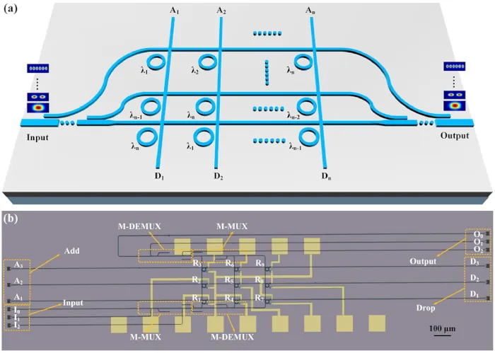
Fig. 1. (a) Schematic of the ROADM for WDM-MDM systems, (b) microscopic image of the manufactured ROADM device.
As proof of concept, we present a ROADM on an SOI platform, as shown in Fig. 1(b). The device is fabricated on an SOI wafer with a 220 nm thick Si top layer and a 3 μm thick buried SiO2 layer. The footprint of the fabricated device is 3 mm × 0.6 mm. Electron beam lithography (EBL) and inductively coupled plasma etching (ICP) processes are used to form the device's waveguides. The radius of the micro-ring waveguides in the switching array is 10 μm, and the radius of other curved waveguides in the (DE)MUXs is also designed to be 10 μm. The device's M-(DE)MUX is based on asymmetric directional couplers (ADCs). According to the phase-matching condition [27], the effective mode index TE0 in a 0.45 μm wide single-mode waveguide is approximately 2.36. Therefore, the widths of the multimode waveguides are determined to be 0.93 μm for TE1 mode coupling and 1.41 μm for TE2 mode coupling. In this work, the coupling gap of the M-(DE)MUX has been designed to be 0.2 μm. To maximize mode coupling efficiency, coupling lengths of 27 μm and 34.5 μm for TE1 and TE2, respectively, are chosen. A 150 μm long adiabatic cone has been designed between waveguides of different widths to reduce crosstalk between modes. In the switching array, the coupling gap between the micro-ring waveguides and the fundamental mode waveguides has been set at 0.15 μm. A 2 μm thick SiO2 layer has been deposited on the waveguides as an insulating layer. To alter the resonant wavelength, a 100 nm thick, 5 μm wide Ti microheater is deposited on each MRR. Twelve grid couplers are integrated into the port terminals (including the add ports, bypass ports, input ports, and output ports) to facilitate communication with external equipment, encompassing optical signal input and output.
The resonant wavelength of each MRR in the switching array can be tuned using the thermo-optical effect [28]. We use λ1, λ2, and λ3, referred to as the three working wavelengths. For simplicity, we designate the channel Cij (i = 0, 1, 2; j = 1, 2, 3) for the wavelength channel (λj) with the TEi mode. By monitoring the operating state of the switching array, the desired signals from the different input channels Cij can be discharged to the corresponding output port Di (i = 1, 2, 3), with each output port capable of discharging three channels. Simultaneously, local signals carried by different wavelength channels can be fed into the switching array via the summing ports, and these local signals, along with other input signals, can be multiplexed to the output bus waveguide via the M-MUX. Each aggregation port Ai (i = 1, 2, 3) can add local signals to three channels on the bus waveguide, so all channels on the bus waveguide can be populated through these three aggregation ports.
To illustrate the function of this device, we show a working wavelength allocation scheme for the switch array. The wavelength allocation scheme and the functions of the different switching units in the switch array are shown in Table 1. Each MRR can add or remove the corresponding channel Cij (i = 0, 1, 2; j = 1, 2, 3). Combining Fig. 1 with this information, it is evident that the MRRs in each row and column of the switch array operate at different wavelengths. This wavelength allocation scheme allows each add port to add three different channel signals to the output bus waveguide, and each remove port to simultaneously remove three corresponding channel signals from the bus waveguide. Taking ports A1 and D1 as an example, when the MRRs R1, R4, and R7 are at their respective operating wavelengths, the signals carried by channel λ1 can be added to channel C21, the signals carried by channel λ2 can be added to channel C12, and the signals carried by channel λ3 can be added to channel C03 via port A1 simultaneously. At the same time, the input signals carried by channels C03, C12, and C21 can be discharged to port D1. Therefore, the proposed device achieves the function of loading multiple channels through one add port and discharging them to one drop port. Since WDM is used, mutual exclusivity of the wavelength signals must be ensured during the loading/discharging process. If we need to upload/download signals with different modes on the same wavelength, time-division multiplexing (TDM) technology can be used for signal processing, which improves transmission efficiency by segmenting time, analogous to the TDM mechanism in passive optical networks.
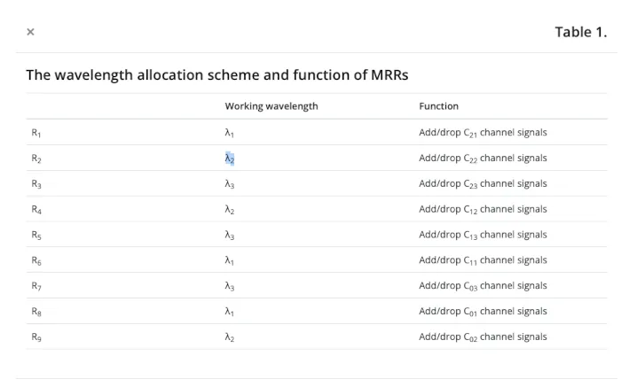
Table 1. Scheme of wavelength allocation and MRR function
3. Experimental Results
Before characterizing the performance of the fabricated ROAMD, we first measured the static spectra of the M-(DE)MUX, which is fabricated on the same chip, as shown in Figure 2(a). An amplified spontaneous emission source (ASE) and an optical spectrum analyzer (OSA) are used to characterize the M-(DE)MUX. The ASE generates broadband light covering the entire C-band. A standard single-mode fiber is used to couple the broadband light to the fabricated device via a grid coupler. Another standard single-mode fiber is used to couple the output optical signals to the OSA. Figures 2(b) to 2(e) show the transmission spectra of the fabricated M-(DE)MUX when light is introduced into port 1, port 2, port 3, and port 4, respectively. The insertion loss (IL) of the manufactured M-(DE)MUX is less than 1.8 dB, while the crosstalk (CT) is less than -15.5 dB in the C-band. The insertion loss of our manufactured device is higher than that of the simulated device, which may be due to EBL instability. In the future, we can design the M-
(DE)MUX with a more robust structure that better meets manufacturing tolerances to reduce the device's insertion loss.
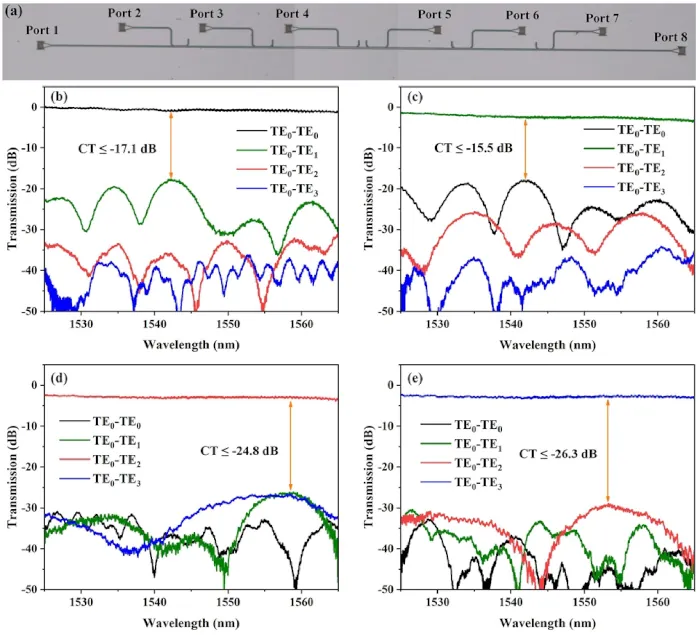
Fig. 2. (a) Micrograph of the fabricated M-(DE)MUX. Static performance of a pair of mode multiplexers with the same structural parameters when the light input is made at port 1 (b), port 2 (c), port 3 (d) and port 4 (e).
Next, we used ASE and OSA to characterize the performance of the fabricated ROADM. By controlling the outputs of the tunable voltage sources (TVS) applied to the microheaters, the state of the switching matrix can be changed. Therefore, a range of response spectra of the fabricated device can be observed through OSA. The operating wavelengths λ1, λ2, and λ3 were chosen to be 1554.5 nm, 1556.0 nm, and 1557.5 nm, respectively. To better describe the device's function, we tested the functions of all the ROADM's add/delete ports, as shown in Figures 3 and 4. Here, we used the transmission spectra of a straight waveguide fabricated on the same chip to normalize the transmission spectra of the fabricated device. The IL of the optical links is less than 7.0 dB, which mainly includes mode coupling loss and crossover loss. The mode coupling losses of the M-(DE)MUX are 0.9–1.0 dB and 0.95–1.1 dB for TE1 and TE2 modes, respectively, when the optical wavelength is 1550–1560 nm. The waveguide crossover loss is 0.4–0.6 dB for the 1550–1560 nm wavelength range. Furthermore, the CT of the manufactured device is better than -13.4 dB.
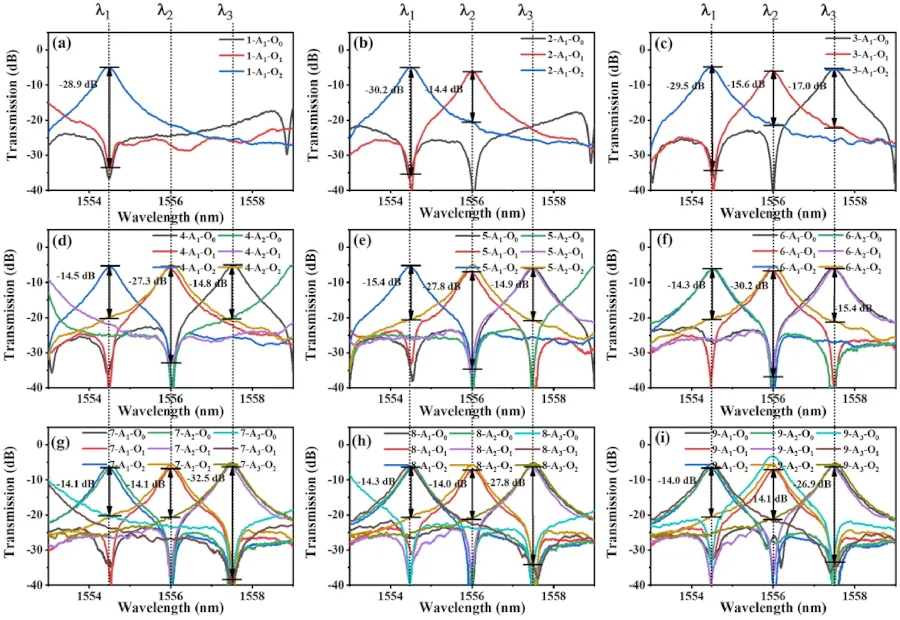
Fig. 3. Static transmissions at output ports (O0-O2) when broadband light is introduced from addition ports (A1-A3).
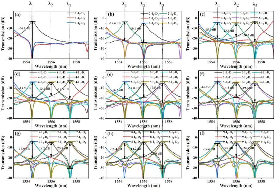
Fig. 4. Static transmissions at the output ports (D1-D3), when the light input comes from the input ports (I0-I1).
In the experimental test, when the resonant wavelength of each MRR is at its operating wavelength, the voltages applied to R1, R2, R3, R4, R5, R6, R7, R8, and R9 are 2.63 V, 1.64 V, 1.72 V, 1.29 V, 2.08 V, 2.01 V, 2.61 V, 3.00 V, and 1.17 V, respectively. The heater resistance is approximately 330 ohms, so the power consumption ranges from 4 mW to 27 mW. Figure 3 shows the insertion ports Ai (i = 1, 2, 3) that load up to three different optical channels into the bus waveguide simultaneously. Conversely, Figure 4 shows the download ports Di (i = 1, 2, 3) that download up to three different optical channels of the bus waveguide simultaneously. When R1, R4, and R7 are at their operating wavelengths, the optical links A1-O2, A1-O1, and A1-O0 are maximal at 1554.5 nm, 1556.0 nm, and 1557.5 nm, respectively, as shown in Figures 3(a)–3(c). Therefore, optical signals of different wavelengths injected from port A1 can be loaded into the corresponding channel of the bus waveguide. In this case, port D1 can download signals into different channels of the bus waveguide simultaneously, as shown in Figures 4(a)–4(c). When R2, R5, and R8 are at their operating wavelengths, the optical links A2-O2, A2-O1, and A2-O0 are maximal at 1556.0 nm, 1557.5 nm, and 1554.5 nm, respectively, as shown in Figures 3(d)–3(f). It can be observed that the optical signals from channels C22, C13, and C01 can be uploaded through port A2. In this case, port D1 can download signals to channels C22, C13, and C01 simultaneously, as shown in Figures 4(d)–4(f). In Figures 3(g) to 3(i), when R3,
R6, and R9 are at their operating wavelengths, the optical links A3-O2, A3-O1, and A3-O0 are at their maximum wavelengths of 1557.5 nm, 1556.0 nm, and 1554.5 nm, respectively. In this state of the switching array, the optical signals from channels C23, C11, and C02 can be fed through port A3. In this case, port D1 can simultaneously discharge signals to channels C23, C11, and C02, as shown in Figures 4(g) to 4(i). Furthermore, to illustrate the switching times of the switching units, we take switching unit R9 as an example. An electrical input signal is applied to switching unit R9 to control the establishment of the optical link for channel C02. Figure 5 shows the output response of channel C02. The result shows that the switching time for add/delete mode operation is approximately 24.0 μs for the rise time and 37.2 μs for the fall time.
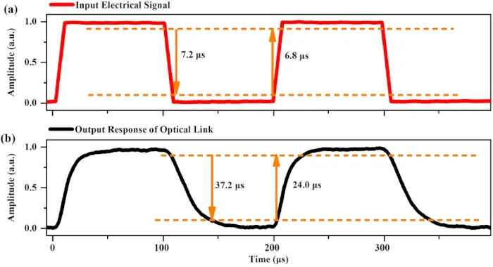
Fig. 5. Measured dynamic response of the MRR to thermal tuning.
Finally, a high-speed data transmission experiment of the fabricated ROADM was conducted. Due to equipment limitations, the ROADM's optical links were tested one by one. Light at a working wavelength corresponding to the optical test link was first generated by a tunable laser (Santec, TSL570) and fed into a polarization controller to ensure the light had TE polarization. The light was then modulated by an electro-optical modulator, which was driven by a 20 Gbps pseudo-random bit sequence with a length of 210⁻¹ generated by an arbitrary waveform generator (Keysight, M8196A). The modulated signal was then fed into the chip and received by a digital communications analyzer (Keysight, 86100D). As shown in Figure 6, the measured eye patterns have an extinction ratio (ER) greater than 11.83 dB, demonstrating that the fabricated ROADM possesses good high-speed communication functionality. To achieve high switching speeds, other advanced modulation technologies, such as the plasma scattering effect [29], can be employed to modulate the switching units.
Fig. 6. Eye patterns measured in the 20 Gbps data transmission experiment for the fabricated ROADM
4. Conclusion
In this article, we have proposed an n×n ROADM for WDM-MDM systems based on a switching matrix on an SOI platform. This allows for the simultaneous reconfiguration of mode and wavelength dimensions through a single add/delete port, offering greater flexibility and efficiency in optical network management. As a proof of concept, we fabricated a 3×3 ROADM device. Experimental results show that each add/delete port can load/unload different signals onto the bus waveguide by controlling the microring array. The IL, encompassing the mode (de)multiplexing components, is less than 7.0 dB, while the ROADM's CT level is better than -13.4 dB, ensuring minimal interference between different channels and maintaining high signal integrity. Finally, the device's high-speed data transmission is demonstrated, and experimental results show that the device supports each add/delete port operating at 60 Gbps (3 × 20 Gbps). Furthermore, the proposed ROADM device exhibits excellent scalability, capable of meeting future data processing demands, making it a powerful and future-proof component in advanced optical communication system architectures.
Funding:
China National Research and Development Program (2022YFB2804202); China National Natural Science Foundation (62405125, W2411059); Gansu Provincial Key Research and Development (24YFGA007); Gansu Provincial Natural Science Foundation (23JRRA1026); State Key Laboratory of Advanced Optical Communication Systems and Networks (2024GZKF12).
Disclosures
The authors declare that they have no conflict of interest.
Data Availability
The data on which the results presented in this article are based are not currently publicly available, but may be obtained from the authors upon reasonable request.
References
1. DAB Miller, “Device requirements for optical interconnects with silicon chips,” Proc. IEEE 97(7), 1166–1185 (2009).
2. RG Beausoleil, PJ Kuekes, GS Snider, et al., “Nanoelectronic and Nanophotonic Interconnect,” Proc. IEEE 96(2), 230–247 (2008).
3. R. Soref, “The past, present, and future of silicon photonics,” IEEE J. Sel. Top. Quantum Electron. 12(6), 1678–1687 (2006).
4. L. Tsybeskov, DJ Lockwood, and M. Ichikawa, “Silicon Photonics: CMOS Going Optical,” Proc. IEEE 97(7), 1161–1165 (2009).
5. D. Liu, M. Zhang, Y. Shi, et al., “Four-channel CWDM (de)multiplexers using cascaded multimode waveguide gratings,” IEEE Photonics Technol. Lett. 32(4), 192–195 (2020).
6. TH Yen and YJ Hung, “Manufacturing-tolerant CWDM (de)multiplexer based on cascaded Mach-Zehnder interferometers on silicon-on-insulator,” J. Lightwave Technol. 39(1), 146–153 (2020).
7. SS Cheung and MRT Tan, “Silicon nitride (Si3N4) multiplexers (de)multiplexers for 1 μm CWDM optical interconnects,” J. Lightwave Technol. 38(13), 3404-3413 (2020).
8. D. Dai, L. Liu, S. Gao, et al., “Polarization management for silicon photonic integrated circuits,” Laser Photonics Rev. 7(3), 303-328 (2013).
9. K. Gallacher, P. F. Griffin, E. Riis, et al., “Silicon nitride waveguide polarization rotator and polarization beam splitter for chip-scale atomic systems,” APL Photonics 7(4), 046101 (2022).
10. J. Zhan, J. Brock, S. Veilleux, et al., “Polarization-independent silicon nitride polarization beam splitter based on MMIs and apodized Bragg gratings,” Opt. Express 29(10), 14476–14485 (2021).
11. Y. He, Y. Zhang, Q. Zhu, et al., “Single-polarization silicon high-order mode (de)multiplexer,” J. Lightwave Technol. 36(24), 5746–5753 (2018).
12. B. Paredes, Z. Mohammed, J. Villegas, et al., “Dual-band (O and C bands) two-mode multiplexer on the SOI platform,” IEEE Photonics J. 13(3), 1–9 (2021).
13. H. Xie, Y. Liu, S. Wang, et al., “Highly compact and efficient four-mode multiplexer based on pixelated waveguides,” IEEE Photonics Technol. Lett. 32(3), 166–169 (2020).
14. Y. Liu, Z. Wang, Y. Liu, et al., “Ultracompact photonic integrated circuit with mode-division multiplexing for dual polarizations,” J. Lightwave Technol. 39(18), 5925–5932 (2021).
15. Y. He, X. Li, Y. Zhang, et al., “On-chip metamaterial-enabled high-order mode-division multiplexing,” Adv. Photonics 5(5), 056008 (2023).
16. OM Nawwar, HMH Shalaby, and RK Pokharel, “Photonic Crystal-Based Compact WDM/MDM (De) Hybrid Multiplexer for SOI Platforms,” Opt. Lett. 43(17), 4176–4179 (2018).
17. X. Fu, J. Niu, Y. Huo, et al., “Polarization-Independent Reconfigurable WDM-MDM Hybrid Multiplexer on Silicon Photonic Platform,” IEEE Photonics Technol. Lett. 35(8), 438–441 (2023).
18. H. Jia, T. Zhou, X. Fu, et al., “Reverse Design and Demonstration of an Ultracompact Silicon Metastructure Mode-Switching Device,” ACS Photonics 5(5), 1833–1838 (2018).
19. X. Han, H. Xiao, Z. Liu, et al., “On-chip reconfigurable mode-switching for optical mode-division multiplexing networks,” J. Lightwave Technol. 37 (3), 1008–1013 (2018).
20. C. Li, H. Zhang, G. Zhou, et al., “Hybrid WDM-MDM transmitter with an integrated Si modulating array and a comb source with a microresonator,” Opt. Express 29(24), 39847–39858 (2021).
21. S. Ohta, T. Fujisawa, S. Makino, et al., “Si-based Mach-Zehnder wavelength/mode multiplexer/demultiplexer for a WDM/MDM transmission system,” Opt. Express 26(12), 15211–15220 (2018).
22. S. Wang, X. Feng, S. Gao, et al., “On-chip reconfigurable add-delete optical multiplexer for hybrid wavelength/mode division multiplexing systems,” Opt. Lett. 42(14), 2802–2805 (2017).
23. Y. Jiang, Z. Zhang, J. Yang, et al., “Reconfigurable flexible add-delete optical multiplexer for mode division multiplexing systems,” IEEE Photonics Technol. Lett. 32(24), 1515–1518 (2020).
24. W. Zhao, Y. Peng, X. Cao, et al., “On-chip reconfigurable 96-channel add-delete optical multiplexer for multidimensional multiplexing systems,” Nanophotonics 11(18), 4299–4313 (2022).
25. X. Yi, W. Zhao, C. Li, et al., “Reconfigurable add-delete optical multiplexers for hybrid mode-division/wavelength-division multiplexing systems,” Adv. Photonics Nexus 2(6), 066004 (2023).
26. W. Bogaerts, PH De, TV Van, et al., “Silicon microslot resonators,” Laser Photonics Rev. 6(1), 47–73 (2012).
27. L.-W. Luo, N. Ophir, CP Chen, et al., “WDM-compatible mode-division multiplexing on a silicon chip,” Nat. Commun. 5(1), 3069 (2014).
28. G. Cocorullo, F.G. Della Corte, and I. Rendina, “Temperature dependence of the thermo-optic coefficient in crystalline silicon between room temperature and 550 K at the wavelength of 1523 nm,” Appl. Phys. Lett. 74(22), 3338–3340 (1999).
29. Q. Chen, F. Zhang, L. Zhang, et al., “1 Gbps directed optical decoder based on two cascaded microslot resonators,” Opt. Lett. 39(14), 4255–4258 (2014).
© 2025 Optica Publishing Group under the terms of the Optica Open Access Publishing Agreement