 In the previous article in this series, we presented different technological options for implementing 3R optical regenerators. Specifically, we studied clock recovery subsystems based on a Fabry-Pérot filter, a PLL, or a self-pulsating laser. These subsystems, in combination with SOA-MZIs, electroabsorption modulators, or semiconductor optical amplifiers, allow us to build high-speed 3R regenerators. To date, countless optical regenerator architectures have been demonstrated. Given the impossibility of studying them all, and considering that they are based on similar operating principles, this article will supplement the analysis with some additional examples. Specifically, we will describe the operation of a fiber-based clock recovery circuit, as well as two 3R regenerators based on SOA and fiber, the latter being suitable for DPSK signals.
Fiber-Based Clock Recovery Circuit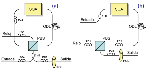 As discussed in previous articles, the key difference between a 2R and a 3R regenerator lies in the clock recovery circuit. Therefore, this type of circuit can be analyzed more or less independently, as it can be applied to a multitude of 2R architectures to achieve 3R optical regenerator functionality. We will now examine an example of a fiber-based clock recovery circuit, which can also be used as a modulator for signal regeneration. Active
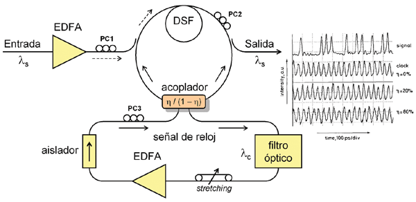
soliton control via synchronous modulation theoretically allows for unlimited transmission distances. Its operating principle is based on periodically remodulating the soliton pulse train to correct temporal jitter. An example of the synchronous modulation technique was covered in the previous article; however, we will now use fiber-based devices. The architecture of this regenerator is shown in Figure 1. This figure illustrates a laser cavity formed by an EDFA, an optical filter centered at the clock signal wavelength, an isolator, and a NOLM (nonlinear optical loop mirror) modulator composed of approximately 10 km of dispersion-shifted fiber (DSF). This type of modulator allows control of the AM/FM modulation process by adjusting the coupling factor of the input divider. The RZ input signal is applied to this modulator via an 80/20 coupler. By adjusting the peak power of this input signal, low-chirp intensity modulation can be achieved. The regenerated output signal is extracted using another coupler. The correct operation of the regenerator depends largely on clock recovery, which in turn depends on the selected coupling factor. Typically, coupling factors around 80% allow for mode locking with AM predominating over FM, thus reducing the generated chirp. Some experimental results of clock recovery for different coupling factors are shown in the same figure (S. Bigo and E. Desurvire, ELL, vol. 31, no. 21, p. 1856), where the influence of the coupling factor is evident.
Polarization-Switching Regeneration in a Sagnac Interferometer.
In this case, the regenerator consists of a four-port polarization beam splitter (PBS), two of which form a fiber loop incorporating a semiconductor optical amplifier (SOA). For the circuit to function correctly, the clock signal must be applied to the PBS input at a 45° angle, splitting it into two orthogonal signals that propagate along the loop in counterpropagation and recombine at the PBS output port (Figure 2). Similar to a TOAD (terahertz optical asymmetric demultiplexer), the SOA is offset from the loop's center point (Conectrónica no. 60, pp. 10-16), so the clock pulses reach the SOA at different times and do not overlap within it. On the other hand, the data signal is coupled to the interferometer synchronized with the clock signal, such that the pulses enter the SOA precisely in the time interval between the two clock pulses. In this way, only one of the clock pulses undergoes intensity modulation and a nonlinear phase shift due to XPM, modifying the polarization state of the clock signal at the PBS output and interfering with the polarizer (POL). The result is a regenerated signal that has been shaped and resampled according to the quality of the clock signal, and in turn modulated with the information encoded in the data sequence.
Depending on how the data signal is applied, the device can function solely as a regenerator (Figure 2a), or simultaneously as a wavelength converter (Figure 2b). In the latter case, the regenerator is insensitive to the polarization of the data signal. In both configurations, a polarization controller (PC1) is used to adjust the optical power of the two clock components propagating through the loop, along with two additional controllers (PC2 and PC3) to compensate for the birefringence of the fiber interferometer. The main advantages of using a Sagnac interferometer as an optical regenerator are its simplicity in controlling the switching window and its stability under temperature changes. Note that the time-switching window can be easily adjusted by controlling the position of the SOA, which in turn can be determined by means of a delay line located in the loop.
Figure 3 shows some experimental results for both regenerator configurations (G. Gavioli and P. Bayvel, PTL, vol. 15, no. 9, pp. 1261–1263). These results were obtained at a speed of 10 Gbit/s, showing a power penalty for a BER = 10⁻⁹ of less than 0.5 dB for the configuration with wavelength conversion, and less than 2 dB for the regenerator without conversion. This increased penalty for the configuration without wavelength conversion is due to internal reflections in the SOA. In any case, the eye diagrams show correct operation in both cases.
DPSK Signal Regenerator.![]() Up to this point, the analysis of regenerators has focused primarily on configurations where the data signal is intensity modulated. However, the use of DPSK signals is beginning to generate increasing interest (Conectrónica no. 114, pp. 8-12), and this is also reflected in the emergence of 3R regenerators adapted to this modulation format. Figure 4 shows the block diagram of one of these regenerators. It consists of a 1-bit delay interferometer (DI), an amplitude regenerator, an optical phase modulator, and a pulsed source with a clock recovery circuit. As can be seen, the architecture is very similar to that seen for other interferometers. In this case, the difference lies in the need for a phase-to-intensity converter at the input (DI) and subsequently a phase modulator at the output. In this way, DPSK signals are transformed into OOK signals, which are regenerated and then re-modulated into DPSK using a phase modulator made with high nonlinearity fiber (HNLF). Similarly, the amplitude regenerator is based on an HNLF, which stabilizes the amplitude of the data pulses by broadening their spectrum and employing selective filtering outside the center frequency. As a result of all this processing, the data encoded in the phase of the output pulses corresponds to the XOR logic function between adjacent bits of the input signal, so some type of decoder will be required at the receiver.
Up to this point, the analysis of regenerators has focused primarily on configurations where the data signal is intensity modulated. However, the use of DPSK signals is beginning to generate increasing interest (Conectrónica no. 114, pp. 8-12), and this is also reflected in the emergence of 3R regenerators adapted to this modulation format. Figure 4 shows the block diagram of one of these regenerators. It consists of a 1-bit delay interferometer (DI), an amplitude regenerator, an optical phase modulator, and a pulsed source with a clock recovery circuit. As can be seen, the architecture is very similar to that seen for other interferometers. In this case, the difference lies in the need for a phase-to-intensity converter at the input (DI) and subsequently a phase modulator at the output. In this way, DPSK signals are transformed into OOK signals, which are regenerated and then re-modulated into DPSK using a phase modulator made with high nonlinearity fiber (HNLF). Similarly, the amplitude regenerator is based on an HNLF, which stabilizes the amplitude of the data pulses by broadening their spectrum and employing selective filtering outside the center frequency. As a result of all this processing, the data encoded in the phase of the output pulses corresponds to the XOR logic function between adjacent bits of the input signal, so some type of decoder will be required at the receiver.
In summary, in this series of articles we have analyzed different 3R optical regenerator architectures. We have described their components and operating principles, also providing experimental results obtained in various laboratories. Although this is still a research topic, some companies have already announced the possibility of this technology becoming available in the short term, as shown in the first article of the series. It is only a matter of time, motivated largely by the continuous increase in bit rate and reach of optical networks.
Francisco Ramos Pascual. Doctor of Telecommunications Engineering.
Full Professor at the Polytechnic University of Valencia.
E-mail: