This increase introduces significant signal integrity issues at the switch socket, motherboard, and edge connector, resulting in higher power dissipation at the SerDes interfaces. In future Ethernet switching, these signal integrity issues could cause I/O power consumption to exceed that of the switch core. Furthermore, the integration density of standard pluggable modules is limited by the QSFP/OSFP form factor, requiring advanced thermal management solutions that are not yet widely available.
Co-packaged optics (CPO) presents a promising solution to these challenges. Unlike traditional plug-in models, CPO integrates optical modules directly into the switch's ASIC substrate, reducing electrical reach and effectively resolving signal integrity issues. This approach has gained traction among leading data centers. However, optimizing the packaging strategy for CPO remains a subject of ongoing discussion and development within the industry. The latest report from IDTechEx, "Co-Packaged Optics (CPO) 2025-2035: Technologies, Market, and Forecasts," explores these advancements in CPO technology and the packaging techniques that enable its adoption.
The importance of advanced semiconductor packaging technologies for co-packaged optics (CPO)
The integration of silicon photonic integrated circuits (CPOs) in data centers aims to increase I/O bandwidth and reduce power consumption. The way photonic integrated circuits (PICs) are combined with electronic integrated circuits (EICs) and switching integrated circuits can significantly influence area and edge bandwidth density, as well as packaging parasitology. These factors directly affect I/O bandwidth and the transceiver's power efficiency, so improper integration can negate the advantages of silicon photonics.
In the case of CPOs, the integration of photonic and electronic components can be achieved through various methods, each with its own unique advantages and challenges. The most advanced, and still in the R&D phase, is 3D monolithic integration. In this method, photonic components are integrated into an existing electronic process node with minimal alterations, placing the active photonics and control electronics on the same die. This reduces parasitic noise and simplifies packaging by eliminating the need for interface pads and protrusions. However, monolithic integration typically uses older CMOS nodes, resulting in suboptimal photonic performance and higher power consumption. Despite these limitations, it offers minimal impedance mismatch and simplified packaging.
In contrast, 2D integration places the PIC and EIC side-by-side on a printed circuit board, connected by wire links or a flip-chip. This method is simple and cost-effective, but it introduces significant parasitic inductance, limiting aggregate I/O due to the single-edge connections. Although 2D integration is easy to package, the reliance on wire junctions limits the transceiver's bandwidth and increases power consumption, making it less efficient for high-performance applications.
3D hybrid integration offers a more advanced solution by placing the EIC directly onto the PIC, using various advanced semiconductor packaging technologies such as TSV (Through-Si-Via), high-density fan-out, Cu-Cu hybrid junction, and active photonic intercalator, which significantly reduces parasitic interference. The use of advanced semiconductor packaging technologies in 3D integration allows for a dense pitch, improving performance. However, heat dissipation remains a challenge, as the heat generated by the EIC can affect the PIC, requiring advanced thermal management solutions. Despite these thermal issues, 3D hybrid integration achieves higher performance thanks to the minimization of packaging parasitic interference.
2.5D integration serves as an intermediate solution, as both the EIC and the PIC are encapsulated in a passive interpolator with TSV. This approach maintains a manageable level of parasitic interference and dense pass capabilities similar to 3D integration, but adds complexity with the need for traces in the interpolator. 2.5D integration balances performance, cost, and manufacturing time, but generates more parasitic interference than hybrid 3D integration.
In summary, each integration method has advantages and disadvantages in terms of performance, complexity, and cost, and the choice depends on the specific requirements and limitations of the application.
Trajectory of the jointly packaged optics (CPO) market
According to IDTechEx, the jointly packaged optics (CPO) market is projected to exceed $1.2 billion by 2035, with robust year-over-year growth of 28.9% between 2025 and 2035. CPO network switches are expected to dominate revenue generation, driven by the ability for each switch to incorporate up to 16 CPO PICs. Optical interconnects for AI systems will constitute approximately 20% of the market, with each AI accelerator typically using an optical interconnect PIC to meet the increasing demand for high-speed data processing and communication in advanced computing applications.
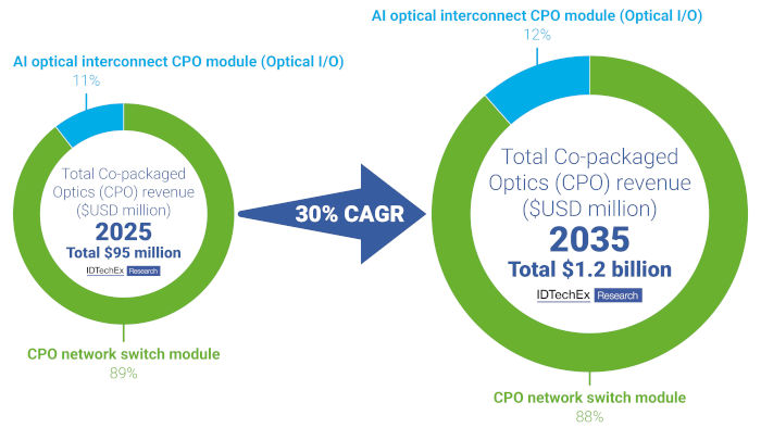
IDTechEx's latest report, "Co-Packaged Optics (CPO) 2025-2035: Technologies, Market, and Forecasts," offers a comprehensive exploration of the latest advancements in co-packaged optics technology. The report delves into key technical innovations and packaging trends, providing an in-depth analysis of the entire value chain. It thoroughly assesses the activities of major industry players and offers detailed market forecasts, projecting how the adoption of CPO will reshape the landscape of future data center architecture.
A central aspect of the report is the recognition of advanced semiconductor packaging as a cornerstone of Co-Packaged Optics technology. IDTechEx places particular emphasis on understanding the role that different semiconductor packaging technologies can play in the field of CPO.
Author: Dr. Yu-Han Chang, Senior Technology Analyst at IDTechEx