To overcome these limitations, the industry is undergoing a paradigm shift. Optical transceivers are moving closer to ASICs, aiming to shorten the copper channel required for electrical signal transmission. However, despite advancements in copper channel length reduction, the challenges posed by deviating from the industry-standard pluggable architecture are not yet fully resolved. Consequently, the industry may be heading directly toward more advanced solutions, such as co-packaged optics (CPO). The IDTechEx report, "Co-Packaged Optics (CPO) 2025-2035: Technologies, Market, and Forecasts," explores the latest developments in CPO technology. It analyzes key technical innovations and packaging trends, assesses major industry players, and provides detailed market forecasts, highlighting how CPO adoption will transform the future architecture of data centers.
The rise of co-packaged optics (CPO)
Co-packaged optics (CPO) represents a significant leap forward in data transmission technology. CPO integrates the optical engine and switching silicon onto the same substrate. This design eliminates the need for signals to traverse the printed circuit board, further reducing the electrical channel path and significantly improving performance.
Reducing the electrical channel path is crucial because the core of data transfer relies on the copper-based SerDes (serializer/deserializer) circuit, which connects the switching ASIC to the pluggable transceivers. As data demand grows, SerDes technology has evolved to enable faster transmission, but faster ASICs require better copper connections, either through more channels or higher speeds. However, as link density and bandwidth increase, a significant portion of system power—and therefore cost—is consumed in driving signals from the ASIC to the optical interconnects at the rack edge. The size limitations of ASIC BGA (ball grid array) packets, due to warping issues, necessitate higher SerDes speeds to support greater bandwidth. However, this also results in higher power consumption, as higher frequencies produce greater channel losses.
One of the key solutions to these challenges is reducing the distance between the ASIC and the optical transceiver. A significant portion of the system's power is consumed in driving data signals from the ASIC to the optical interconnects at the rack edge. Bringing the optical transceivers closer to the ASIC offers several advantages:
Reduced signal loss: Shortening the electrical path between the ASIC and the optical interconnect minimizes signal degradation.
Lower power consumption: Reducing the distance allows the use of lower-power SerDes options, resulting in lower overall system power consumption.
Increased efficiency and performance: By reducing the power required for data transmission, system efficiency and performance are significantly improved.
Scalability: CPO technology supports future scalability of high-bandwidth systems, making it ideal for data centers that need to meet increasing data demands.
How the CPO will shape the interconnection architecture for AI
The CPO is poised to transform the interconnect architecture for AI. In this article, IDTechEx uses Nvidia's cutting-edge DGX NVL72 server as an example to explain how IDTechEx envisions the next-generation AI architecture. Nvidia, the market leader in AI accelerators, designed the DGX NVL72 to redefine AI performance standards, supporting up to 27 trillion parameters, far surpassing ChatGPT 4's 1.5 trillion parameters.
The DGX NVL72 contains 18 compute nodes, each equipped with four Blackwell GPUs and two Grace CPUs, along with nine NVLink switches. Modern AI accelerator architectures like this one employ multiple communication networks to manage data flow:
Backside Compute Network: In the DGX NVL72 architecture, each compute node connects to an L1 compute switch via Nvidia's NVLink Spine, a high-speed copper interconnect that delivers 1.8T of bidirectional bandwidth across 18 lanes of 100G, using 36 copper wires per connection. The L1 switches are similarly interconnected, resulting in a total of 5,184 copper wires across the entire system. To maintain signal integrity over these distances, timers are used in the switches, although these introduce latency and bandwidth limitations, especially at higher speeds like 100G per lane. Furthermore, while cost-effective, copper links suffer from signal degradation issues such as channel loss and clock jitter over long distances, which become more pronounced as bandwidth demands increase.
Optical interconnects offer a compelling alternative to copper, providing significantly higher bandwidth density and greater efficiency over long distances—critical for AI workloads involving massive data transfers between GPUs. Looking ahead, copper interconnects are expected to be replaced by co-packaged optical (CPO) interconnects, enabling direct connections between compute nodes and eliminating the need for L1 compute switches in the backbone network.
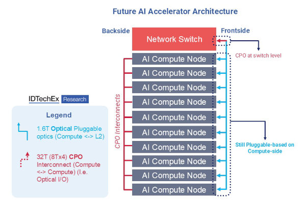
Ultimately, the CPO will reshape the AI interconnect architecture, improving data flow, reducing bottlenecks, and enabling greater efficiency and scalability in next-generation AI systems. We will likely see direct optical connections in the future, eliminating compute switches and increasing bandwidth for AI workloads, although this will also increase the complexity of those connections.
A central aspect of the report is the recognition of advanced semiconductor packaging as a cornerstone of co-packaged optics technology. IDTechEx places particular emphasis on understanding the role that different semiconductor packaging technologies can play in the field of CPO.
Author: Dr. Yu-Han Chang, Principal Technology Analyst at IDTechEx