 Question: What is an RF attenuator and how do I select the right one for my application?
Introduction
To continue the series of short articles on RF for non-RF engineers, we will discuss attenuator ICs and provide some insights into their types, configurations, and specifications. This article aims to help engineers get started with a wide variety of IC products and choose the right one for a given application. Other articles in this series include: “A Guide for Choosing the Right RF Amplifier for Your Application,” “How to Easily Select the Right Frequency Generation Component,” and “RF Demystified—Understanding Wave Reflections.”
Types of Attenuators
From a key functional perspective, attenuators can be classified as fixed attenuators with an invariable attenuation level and variable attenuators with an adjustable attenuation level. Based on the attenuation control method they support, variable attenuators can be further classified as voltage variable attenuators (VVAs), with analog control, and digital step attenuators (DSAs), which are digitally controlled.
VVAs provide continuous adjustment of attenuation levels, which can be set to any value within a given range. Analog variable attenuators are typically used for automatic gain control circuits, calibration corrections, and other processing functions where smooth and precise signal control is required.
DSAs feature a set of discrete attenuation levels that allow the signal strength to be adjusted with a predetermined attenuation step size. Digitally controlled RFIC attenuators offer a microcontroller-compatible control interface and are a good solution for maintaining functional integrity in complex designs.
 Design Configurations.
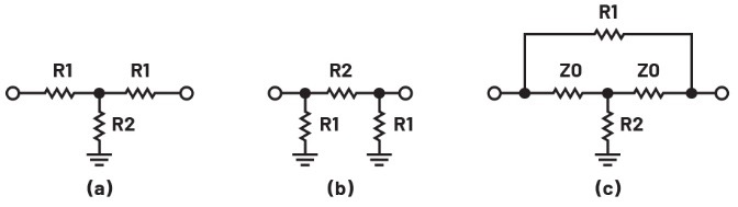
Attenuator integrated circuits can be implemented in GaAs, GaN, SiC, or CMOS technologies using resistors, PIN diodes, FETs, HEMTs, and CMOS transistors. Figure 1 shows three basic topologies underlying various attenuator design configurations: T-type, π-type, and bridged T-type networks.
Fixed-value attenuators utilize these basic topologies implemented with resistors in hybrid thin- and thick-film technologies to provide fixed attenuation levels.
VVAs typically use a T-type or π-type configuration with a diode or transistor element operating in a nonlinear resistance region. The resistance characteristics of the base elements are exploited to adjust the required attenuation level by varying the control voltage.
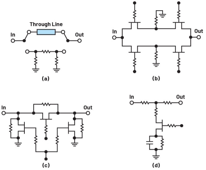
DSAs typically employ several cascaded units representing individual bits that can be switched on or off to achieve the necessary attenuation level. Figure 2 shows some examples of configurations used for DSA designs. These include configurations with integrated SPDT switches that toggle the input and output ports with the attenuator pickup and a pass-through line, switched device designs with transistors or diodes used as switchable resistors, switched resistor configurations where the resistors can be switched in or out of the circuit, and integrated device-type designs with a transistor or diode as an integral part of the design.
 Attenuator topologies can be arranged in either a reflection or balanced/balanced design, as shown schematically in Figure 3. Reflection-type devices use attenuators of equal strength, as do balanced-type devices. Reflection-type devices use identical attenuators connected to the output of a 3 dB quadrature coupler and typically offer a large dynamic range. Balanced configurations combine a pair of identical attenuators using two 3 dB quadrature couplers and provide good VSWR and power handling capability.
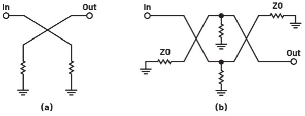 Besides the main design configurations described in this article, other circuit types exist for implementing attenuator IC components; however, their consideration is beyond the scope of this brief article.<sup>1,2</sup>
Key Specifications
► To select the appropriate type of attenuator for the final application, the engineer must have a thorough understanding of its key specifications. Besides attenuation capabilities and some fundamental parameters such as insertion and return losses, there are several other characteristics used to describe attenuator components, the key ones of which include:
► Frequency range (Hz): the frequencies across which the IC maintains its specified characteristics.
► Attenuation (dB): the amount of suppression above the insertion loss.
► Frequency response: variation of the attenuation level (dB) across the frequency range (Hz)
► Attenuation range (dB): total attenuation value provided by the component
► Input linearity (dBm): usually expressed in terms of the third-order intercept point (IP3), which defines a hypothetical point for the input power level at which the power of the corresponding spurious components would reach the same level as the fundamental component
► Power handling (dBm): usually described in terms of the 1 dB input compression point, which defines the input power level at which the insertion loss of the attenuator decreases by 1 dB; the power handling characteristic is usually specified for average and peak input power levels for steady-state and hot-switching modes.
Relative phase (degrees): phase shift introduced into a signal by the attenuator component.
In addition to these common parameters, variable attenuators are also described by their switching characteristics, which are usually expressed in ns in terms of rise and fall time, turn-on and turn-off time, and the time it takes for the RF output signal to reach amplitude and phase.
There are also specific characteristics inherent to each type of variable attenuator.
In the case of VVAs, these are related to their analog control operation and include:
► Voltage control range (V): the voltages required to adjust the attenuation level within the attenuation range.
► Control characteristics, generally expressed in terms of the attenuation slope (dB/V) and performance curves that show the attenuation level as a function of the control voltage.
In the case of DSAs, their inherent characteristics include:
► Attenuation accuracy (also known as state error) (dB): the limit of variation of the attenuation level from the nominal value.
► Attenuation step size (dB): the difference between any two successive attenuation states.
► Step error (dB): Limit of variation of the attenuation step size with respect to the nominal value
► Overshoot, undershoot (dB): Level of signal transients (glitches) during state transitions.
Generally, a good attenuator component is required to offer flat attenuation performance and good VSWR across the entire operating frequency range, to offer sufficient accuracy and power handling capacity, and to ensure smooth, glitch-free operation with little signal distortion during state transitions or to provide a linear control characteristic.
Conclusion:
The wide variety of attenuator IC components is not limited to those discussed in this article. Other types of ICs include frequency-dependent and phase-compensated attenuators, temperature-dependent variable attenuators, programmable variable variable attenuators (VVAs) with an integrated DAC, and others. However, in this article, we considered the most common categories of attenuator ICs and discussed their main topologies and key specifications, which can help an RF designer choose the right component for a given application.
Analog Devices offers the broadest portfolio of integrated RF components in the industry. ADI attenuator ICs are available in a wide range of architectures and form factors, giving designers the flexibility to select the component that best suits their system requirements.
The components are designed to deliver best-in-class performance and highly reliable operation to meet the most demanding requirements in a wide range of applications in the instrumentation, communications, military, and aerospace markets.3
References
1Inder J. Bahl. Control Components Using Si, GaAs, and GaN Technologies. Artech
House, 2014.
2Ian Robertson and Stepan Lucyszyn. RFIC and MMIC Design and Technology.
The Institution of Engineering and Technology, November 2001.
3“RF, Microwave, and Millimeter Wave Products Selection Guide 2021.” Analog Devices, Inc., September 2021.
About the author:
Anton Patyuchenko is an RF specialist with over 15 years of experience in this field. He graduated with a degree in Microwave Engineering from the Technical University of Munich in 2007. After graduation, Anton worked as a research associate at the Institute for Microwave and Radar at the DLR. In 2015, he joined Analog Devices and currently holds the position of Technical Lead, Field Applications, with a focus on RF technologies.