 Designed for printed circuit board (PCB) mezzanine applications in corporate network towers and telecom hubs and servers, as well as for industrial controllers and high-capacity scanners for medical and military purposes, the NeoScale mezzanine interconnect features a patent-pending wafer triad configuration that isolates each differential pair to achieve optimal levels of performance and customization.
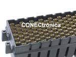
The honeycomb structure of the NeoScale mezzanine interconnect housing minimizes crosstalk in each triad by directing it out of the PCB by one or two layers, resulting in significant PCB material savings for designers. Furthermore, the unique honeycomb structure within the connector housing protects the mating interface and flexible contacts, helping to prevent terminal damage. With a density of 82 differential pairs per square inch, the NeoScale interconnect layout can be customized with high-speed differential pairs, high-speed single-terminate traces, low-speed single-terminate traces, and power contacts. Available in 85 Ω and 100 Ω impedances and stacking heights from 12 mm to 40 mm, NeoScale design options include 6 to 30 circuit column sizes with 2, 4, 6, and 8 row options, spanning 12 to 240 triads in a single assembly.
The NeoScale mezzanine interconnect utilizes Molex's patented Solder Charge Technology™ as a fixturing method for PCB terminations. A more cost-effective and reliable alternative to BGA (Ball Grid Array) connections, the surface mount technology (SMT) simplifies design, facilitates strong solder joints in mass production, and eliminates the need for thermal bonding and complex solder tail shapes.
The NeoScale patch assembly features a 2.80 mm pitch between differential pairs. The patch assembly pin includes bias and modulation functions. The ground pin has two SMT fixing points, with four solder joints per triad, and the PCB footprint remains unchanged when mixing and matching different high-speed, single-terminate differential pairs and power triads within the housing. The NeoScale patch system orientation features a mirrored configuration with a back-to-back shielding divider line. The resulting line of symmetry bisects the triad pair to facilitate PCB routing and pin-out assignment, promoting optimal signal integrity and excellent mechanical stability. These characteristics are further enhanced by the robust molded construction, which protects against damage from handling.