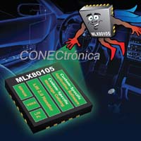
 Melexis expands its family of intelligent LIN slave ICs with a new generation of reconfigurable LIN switching slaves. The LIN bus standard and its SAE J2602 version are experiencing rapid growth in automotive networking due to the protocol's cost-effective and robust nature and its compatibility with CAN bus. The MLX80105 connects any door, roof, seat, steering wheel, instrument panel, HVAC, lighting control, or similar switching module that requires easy access via LIN.
By incorporating the Melexis LIN transceiver's physical layer, Melexis LIN ASSPs (Application Specific Standard Products) guarantee world-leading integrated ESD protection. The LIN protocol processor complies with all LIN standards, including LIN2.0, LIN2.1, and SAE J2602.
The MLX80105 is a fully integrated LIN slave on a single chip. All necessary components—physical layer LIN transceiver, LIN controller, voltage regulator, and application controller—are integrated, along with ADC support, PWM generation, and high-voltage I/O. This high level of integration drastically reduces the BOM and enables the development of very compact and small LIN slave modules.
The well-established Melexis dual-tasking microcontroller, a proven LIN driver, is used to allow application development to be completely decoupled from LIN network load considerations. Application software tasks are handled by a 16-bit RISC microcontroller.
A complete C-based development environment is provided. Low-level LIN driver and software library functions are reused, along with software development in an IDE from the readily available MLX80104 uniROM IC. New customers will find an easy and fast path to application development and deployment, while existing MLX80104 customers can seamlessly integrate the MLX80105 into new or existing projects.
The MLX80105 consumes 50µA of current in sleep mode and can be woken up via the LIN bus, as well as through connected switches or other wake-up sources. The LIN slave supports switches in matrix switching configurations and single switches connected to the 18 available I/O pins. All I/O pins are high-voltage resistant to safely withstand remote connections from a powered-off module. Rotary encoders are supported via eight interrupt-capable I/O pins. Position control and monitoring for dials and control knobs, motors, or actuators are radically simplified with the added advantage of software control and direct physical input, or the ability to share signals between different systems. Analog inputs can convert any analog signal, such as resistive encoders and resistive switches, into BUS messages for use with networked devices. An internal battery monitor enables the use of mains-powered functions.
To illuminate the switching module panel, eight open-drain PWM outputs are provided with a configurable PWM base frequency from 45 Hz to 45 kHz. With a message from the master LIN, the LED output intensity can be adjusted according to specific OEM requirements.
All the aforementioned functions are implemented on a single silicon chip in a 5x5 mm QFN package. This, along with a minimum of external components, allows for the application of a LIN slave in a very small PCB footprint.