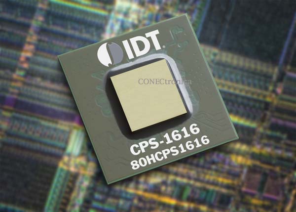
This article details some design methods used to develop a 240 Gbps Gen2 digital switching fabric along with analog serializers and deserializers (SerDes) and high-speed encapsulation, in order to meet the demanding performance requirements of the Serial RapidIO Gen2 specification; and to ensure that the high-speed analog circuitry does not impact the high-performance digital core (or converse) of the Gen2 devices. Some use case implications resulting from switching to SerDes with Serial RapidIO Gen2 performance are also explained.
Physical Layer Enhancements Serial RapidIO Gen2
The Gen2 physical layer specification includes new 2x, 8x, and 16x port lane widths to complement the 1x and 4x widths of the Gen 1 specification. Many endpoint devices and switches available on the market support 4x, 2x, and 1x ports for up to 20 Gbps of raw throughput, which is more than double the capacity of 10 Gb Ethernet solutions and exceeds PCI Express Gen2 by 25%.
The Serial RapidIO Gen2 specification covers all classic electrical specifications for short-, medium-, and long-range transmitters and receivers, including eyemasks where applicable. The Gen1 specification did not require any equalization, but some vendors chose to implement it. However, the Gen2 specification requires equalization at 6.25 Gbaud for any range. At 5 Gbaud, it will likely be necessary for long distances and optional for short and medium distances. For long-range 6.25 Gbaud applications, no eyemask is specified for the receiver because there may not be an "eye" at the end of the channel. This certainly impacts the user's ability in the lab to determine the signal integrity seen at the receiving device.
 The Serial RapidIO specification does not require generating or checking SerDes patterns (for example, transmitting a pseudorandom binary sequence [PRBS] pattern and checking it at the receiver), but some device vendors utilize this proprietary functionality. A new BER characterization feature in the Serial RapidIO Gen2 specification is the 8b/10b per-way decoding error counter. While multibit errors in a given code group cannot be counted, errors logged at this level would likely indicate a severely degraded line. In contrast, this counter is a very reliable indicator of the actual BER of reasonably effective lines with a BER of approximately 10⁻⁹ or better.
SerDes: equalization, integrated ODS (On-Die Scope) indicator, BER testing.
IDT, the leading provider of Serial RapidIO switches, has just announced the availability of the second-generation (Gen2) CPS-1848 and CPS-1616 switches. To meet the high demands of the Serial RapidIO Gen2 specification, IDT has designed a 6.25 Gbaud receiver that utilizes a continuous-time equalizer (CTE) and a decision feedback equalizer (DFE).
The CTE provides a simple zero to increase the amplification of the relevant frequency (i.e., half the baud rate). This is active amplification, although it is performed passively on all received bits. This boost in a specific band improves the gain of the received signal while minimizing noise.
In addition, a five-lead DFE was used, which allows for highly selective gain control while minimizing noise when boosting signals. The DFE compensates for inter-symbol interference (ISI), that is, the negative impact that previously transmitted bits have on each new bit. The DFE actively examines the register of previously transmitted bits (in this case, up to four previous bits) and provides feedback on how to boost each bit. In this way, the receiver can eliminate the effect of ISI frequencies, which would otherwise interfere with the next incoming signal.
 Numerous implementations and design features have been developed to minimize power consumption. The transmitter, for example, offers a high degree of pulse control (pulse strength and pre-emphasis). The user does not have to meet standard requirements at the expense of BER. In the receiver, a half-speed clock enables considerable power savings. This architecture splits the received data path into even and odd bits and then takes full advantage of a half-speed clock. Indeed, the DFE circuitry has also been designed to support this half-speed clock and split data path architecture. The DFE includes features to minimize power consumption, allowing the user to turn off unused taps.
To minimize noise in the SerDes, decoupling capacitors were used to occupy all available space on the chip, thus reducing noise from the digital logic circuits. A differential clock distribution was also employed for the reference clock in all phase-locked loops (PLLs) of the device, as well as in the PLL circuitry on each via. The differential clock distribution improves clock noise immunity. Additionally, the SerDes was isolated by physically separating it from the digital core, and digital switching noise was minimized in the analog circuitry.
Ensuring a suitable high-speed signal up to the package...
At 6.25 Gbaud, channel design and engineering become increasingly important and are directly related to the transceiver. In fact, at this speed, the Serial RapidIO Gen2 specification refers to StateEye-compliant transceivers and channels. A StateEye-compliant transceiver can be designed against a StateEye-compliant channel model, and vice versa. The channel and transceiver are inseparable in terms of specification compliance.
This has ramifications all the way to package design. IDT has designed FCBGA (Flip Chip Ball Grid Array) packages for switches that meet the specification requirements; the package itself is part of the channel, and its design was carried out in coordination with the chip itself, minimizing BGA trace lengths, carefully forming via pairs, and achieving its characteristic impedance.
 To prevent transmitted signals from rejoining the receiver's paths, the CPS-1848 has ground isolation pins between the Tx and Rx pins (see Figure 2). Additionally, the power supply pins divide each path to reduce coupling between paths. The power supply/ground loop inductance is minimized by providing a checkerboard-pattern core voltage (Vdd) and ground connection. This makes it easy to apply decoupling capacitors to the secondary side of the printed circuit board.
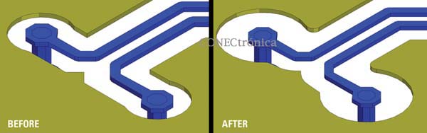
To improve signaling for high-speed Serial RapidIO lines, anti-pads are used to clear the via pad of the signal from the ground plane on the same layer as the pad. To eliminate excessive capacitance, the anti-pad clearance for the laser via pad is increased from 50 µm to 100 µm, and for the core via pad, from 100 µm to 150 µm (see Figure 3), which can improve, for example, the return loss by 12.5 dB at 5.0 GHz.
To minimize noise from the digital core in the high-speed SerDes and PLL, the device and package separate the analog and core power rails. According to the device datasheet, the printed circuit board designer must keep these rails separate. A dedicated SerDes transmitter power supply (Vddtx) operates at 1.2 V, even though the device is manufactured using a 1.0 V core process. This 1.2 V supply voltage ensures strong transmission drive to guarantee that the Serial RapidIO transmitter specifications are exceeded.
Reflections on Use with This Performance:
As mentioned earlier, in the case of long-range transmission at 6.25 Gbaud, there may not be an eye to point at the receiver. At these lane speeds, oscilloscopes costing $100,000 or more would typically be needed to verify signal integrity. Furthermore, receiver equalization can improve the signal seen at the receiver. In fact, what the oscilloscope perceives as external to the device may be much worse than what the chip itself perceives after equalization. With receiver equalization, the ODS becomes a very useful tool for seeing what the device sees. All IDT Gen2 switches use one ODS per lane, which is pattern-independent. Therefore, it works with any arbitrary pattern, including the PRBS-31 test patterns defined in the Serial RapidIO specification, as well as the Serial RapidIO runtime protocol while packets are traversing the links. The ODS is fantastic for quickly optimizing transmission and reception parameters, including equalization, simply by ensuring optimal eye aperture.
A PRBS-31 test pattern can be an ideal and rigorous way to characterize the channel, but it has a wider bit transition spectrum than what would be seen with the standard Serial RapidIO protocol at runtime. As mentioned earlier, the Serial RapidIO specification does not require PRBS pattern generators or testers. The runtime BER in the Serial RapidIO system will be lower than what would be seen using the PRBS pattern. The runtime system BER is undoubtedly best determined using the 8b/10b decoding error counters of Serial RapidIO Gen2.
In conclusion,
the Serial RapidIO Gen2 devices double the port speed to 20 Gbps and are designed for demanding carrier-grade backplane applications. Key to achieving this performance is the enhanced SerDes, which supports up to 6.25 Gbaud and incorporates additional DFE and equalization circuitry. Vendors must synchronize the analog and digital components of their chips, as well as the package itself, to ensure these speeds are easily met.
With double the line speed and the equalization required at these speeds, users may experience a paradigm shift in their use of these devices and in the characteristics of the transceivers and channels. New vendor-specific features, such as ODS and standard BER counters, will aid in this transition and will undoubtedly contribute to easier work in the lab compared to other products.
The author
 Trevor Hiatt is a product manager in the IDT Communications division. His responsibilities include defining strategic products, managing programs, and marketing Serial RapidIO products. Trevor holds a degree in Electrical and Computer Engineering from the University of California, Santa Barbara. For more information, please contact Trevor Hiatt at: