Currently, HBM modules must be packaged with GPUs because the GPU-memory electrical interconnect is limited to a few millimeters in length. The next generations of HBM will require interconnect densities on the order of 10 Tbps/mm or higher. Conventional optical interconnects based on VCSELs or silicon photonics (SiPh) promise to extend the interconnect reach, but they struggle to meet the requirements for size, bandwidth density, power, latency, operating temperature, and cost. In contrast, Avicenna's microLED-based LightBundle interconnects offer higher bandwidth density, a much smaller size, significantly lower power and latency, and very low costs.
“At Avicena, we are delighted to introduce the world’s most compact 1Tbps transceiver in the form of a 3 mm x 4 mm CMOS ASIC utilizing our proprietary microLED optical interface,” says Bardia Pezeshki, founder and CEO of Avicena. “Everyone is talking about SiPh solutions for AI cluster applications. However, for short-range interconnects with a range of less than 10 m, we believe our LED-based solution is inherently better suited due to its compact size, higher bandwidth density, lower power and latency, and tolerance to temperatures up to 150 °C.”.
“Optical interconnect technology has the potential to improve performance between chips and behind the scenes,” says Marco Chisari, head of Samsung’s Semiconductor Innovation Center. “With a roadmap toward multi-Tbps capacity and sub-pJ/bit power efficiency, Avicenna’s innovative LightBundle interconnects can enable the next era of AI innovation, paving the way for even more capable models and a wide range of AI applications that will shape the future.”
About technology
Today's high-performance integrated circuits use electrical interfaces based on SerDes to achieve adequate off-chip density. However, the power consumption and bandwidth density of these electrical links degrade rapidly with length. Conventional optical communication technologies developed for networking applications have proven impractical for inter-processor and inter-processor-memory interconnects due to their size, low bandwidth density, high power consumption, and high cost. The typical need for external laser sources (ELS) with SiPh further increases complexity and cost. In contrast, the LightBundle™ interconnect architecture is based on arrays of innovative GaN microLEDs that leverage the microLED display ecosystem and can be directly integrated into compact, high-performance CMOS integrated circuits. This enables dense, low-power I/O across the entire IC area, allowing for unprecedented chip densities. Each microLED array is connected via a multi-core fiber cable to a corresponding array of CMOS-compatible PDs.
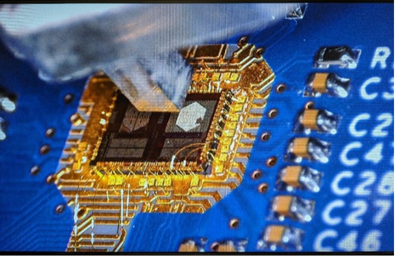
“We have already demonstrated microLEDs transmitting at over 10 Gbps per lane and a test ASIC on a 130 nm CMOS process running 32 lanes at less than 1 pJ/bit,” says Rob Kalman, co-founder and CTO of Avicenna. “Now we are introducing our first ASIC with over 300 lanes and an aggregate bandwidth of over 1 Tbps bidirectional at 4 Gbps per lane. The ASIC measures less than 12 mm² and contains a complete transceiver, including circuitry for the Tx and Rx optical arrays, as well as a high-speed parallel electrical interface and various DFT/DFM functions such as BERT, loopbacks, and Open Eye Monitoring (OEM). All key features of the ASIC have been verified, and we are currently working on performance enhancements for manufacturing scalability.”.
The modular LightBundle platform scales to interconnects with tens of Tbps and a throughput density > 10 Tbps/mm. LightBundle is not tied to any foundry process, allowing it to be integrated into a wide variety of IC processing nodes. Its compact size, high density, low power consumption, and low latency make LightBundle ideal for high-density chip interfaces such as UCIe, OpenHBI, and BoW, and it can also greatly extend the reach of existing computing interconnects such as PCIe/CXL and HBM/DDR/GDDR memory links.