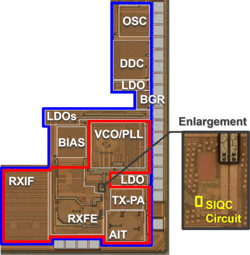
In addition to being compact, low-cost, and energy-efficient, IoT devices must offer flexible Bluetooth LE compatibility regardless of their implementation format. Renesas has developed two new technologies to address these requirements: 1) an impedance matching circuit technology that covers a wide range of impedances and allows the IC to match a variety of antenna and board impedances without an external impedance matching circuit; 2) a signal correction technology for locally generated reference signals that uses a small circuit to self-correct inconsistencies in circuit elements and variations in environmental conditions without requiring calibration.
Renesas has verified the effectiveness of these technologies in a prototype Bluetooth LE RF transceiver circuit built using a 22 nm CMOS process. With these new technologies, Renesas has reduced the circuit area, including the power supply, to 0.84 mm², the smallest in the world for a device of this type. This was achieved by modifying the receiver architecture to reduce the number of inductors and introducing improvements such as a low-current baseband amplifier with a small footprint and a highly efficient Class D amplifier. They offer best-in-class power efficiency, consuming only 3.6 mW and 4.1 mW during reception and transmission, respectively. These advancements allow for a reduction in board size, cost, and power consumption, as well as simplifying the board design process.
The advantages of new RF transceiver technologies are: 1. Matching circuit technology that covers a wide range of impedances (on-chip antenna impedance tuner, AIT)The integrated impedance matching circuit technology presented by Renesas at ISSCC 2015 enabled the creation of compact, low-cost Bluetooth LE products that did not require external inductors or capacitors for switching between receive and transmit modes or for impedance matching. However, depending on the antenna type or board design considerations, the impedance did not necessarily reach 50 Ω, and an external matching circuit was still required. Furthermore, when using the previous technology and adding a matching circuit with impedance-switching functionality, issues related to increased signal loss and the inability to achieve a sufficient variation range could still arise.
To address these issues, Renesas has developed a novel variable impedance matching circuit technology consisting of two inductors and four variable capacitors. The transmitter-side and receiver-side inductors used in the matching circuit are configured concentrically, and their mutual induction is employed to reduce signal loss and trim the effective parasitic capacitance. This widens the variable impedance range and significantly reduces the circuit area. A voltage standing wave ratio (VSWR), which indicates impedance mismatches, equivalent to a maximum of 6.8 has been confirmed, with a variable impedance range of approximately 25 to 300 Ω.
2. Reference signal self-correction circuit technology that eliminates the need for a calibration circuit (IQ phase self-correction, SIQC)The RF transceiver internally generates a reference signal (a locally generated signal) at approximately the same frequency as the wireless radio signals received through the antenna. This signal is used to convert the gigahertz wireless signals into low-frequency baseband signals. The accuracy of the reference signal can be degraded by factors such as inconsistencies in circuit components or variations in temperature or supply voltage. In the past, phase and amplitude offset compensation technology using a calibration circuit was used to accurately generate the reference signal. However, this presented problems, as integrating such a calibration circuit required a larger chip area, increased power consumption, and raised testing costs.
Renesas solved these problems by developing a new phase self-correction circuit technology that uses reference signals from four different phases to correct each other, allowing phase differences to cancel out. This self-correction circuit is much smaller and can be implemented in approximately one-twelfth the size of a conventional calibration circuit. The image signal rejection ratio, crucial for reception performance, averages 39 dB, which meets the Bluetooth standard with a comfortable margin to spare.