As communication speeds approach the Gb/s range, digital engineers are compelled to learn that frequency-domain measurements provide valuable information about time-domain behavior. Similarly, RF and microwave engineers are increasingly working as signal integrity engineers in digital applications. This requires the ability to perform time-domain measurements. This article will explore the relationship between signal measurements in one domain and observations in the other. Valuable data and information regarding the basis bit error rate will be analyzed.
It is rare for an electrical engineering student to graduate with extensive knowledge of both digital electronics and RF and microwave theory. The junior engineer specializing in digital design likely chose that specialization because they want to work with computers. As a rule, the student specializing in high-frequency engineering has a predilection for radio communications, which they cultivated before starting their university studies. The typical electrical engineering degree usually includes some courses covering both digital electronics and RF and microwaves. However, when it comes time to specialize, choose elective courses after completing the introductory ones, and prepare for their future career, each student is likely to choose a distinctly different path. One path leads to the world of Boole and Karnaugh maps, while the other leads to that of Maxwell and Smith.
For many, as they advance professionally, these paths begin to converge. As standard computer serial buses reach transmission speeds of two, five, and even more than ten Gb/s, it's easy to argue that a convergence is occurring between the digital world and the world of RF and microwaves. What does this mean for microwave engineers? Although they transmit simple zeros and ones, their knowledge of fields such as transmission lines, noise processing, phase-locked loops, and communications theory is essential for designing functional digital communications systems. For the digital engineer, their knowledge of digital logic, data encoding, error detection, and recovery remains critical. Now, instead of using that knowledge in security applications or with data corrupted by storage media errors, it's being applied to communications schemes where the transmission channel, used at high speeds, can degrade signals even when the separation between the transmitter and receiver is less than a meter.
What factors can make a high-frequency engineer better prepared for a world of digital communications? And, conversely, why might a digital engineer be more effective when their “bits” contain microwave signal content? One of the skills that allows both engineers to delve into each other’s world is their ability to think in both the time and frequency domains. Observing a digital bitstream on an oscilloscope with some intuition about its frequency-domain equivalent can provide valuable information about the integrity (or lack thereof) of that signal. Measuring the frequency response or bandwidth of a communications channel and anticipating how the shape of the bits will be affected (over time) can help determine the viability of that channel.
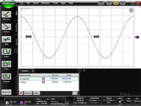
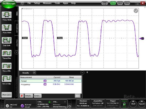
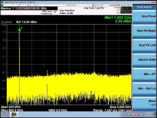 An electrical signal can be displayed as a voltage waveform over time. This is how signals are viewed on an oscilloscope. The signal can also be viewed in a power-over-frequency format. This is how a spectrum analyzer would display it. From a mathematical perspective, time and frequency signals are related by the Fourier transform. The Fourier transform takes a signal/function from the time domain and transforms it into the frequency domain. It indicates which frequencies are present in the waveform in the time domain. Simple examples of this are sine and square waves. Let's take a sine wave with a period of 1 ns (Figure 1A). What frequencies are present in this signal? It's quite simple. There is only one frequency present, a single tone at 1 GHz (Figure 1B). What about a square wave with a period of 1 ns? One might expect it to also have signal content at 1 GHz. However, it is evident that there is more spectral content in this signal than in the sine wave with the same period. In addition to the 1 GHz tone, there is also energy at 3 GHz, 5 GHz, 7 GHz, etc. (Figures 1C and D). The signal consists of a tone at the fundamental frequency (the inverse of the signal period) and its odd harmonics. However, as the frequency of the harmonic tones increases, their amplitudes decrease. As signals in the time domain become more complex, so does their spectrum in the frequency domain. For example, a 2 Gb/s digital data stream will have a spectrum that follows a function (sin x)/xy, unlike the previous examples; it will not have signal content at 2 GHz or 2 GHz harmonics (Figures 1E and F). Note that the 1 GHz square wave is the equivalent of a 2 Gb/s signal transmitting a 1-0-1-0-1-0 pattern, and that the spectral zeros for the square wave and "real" digital communications are identical.
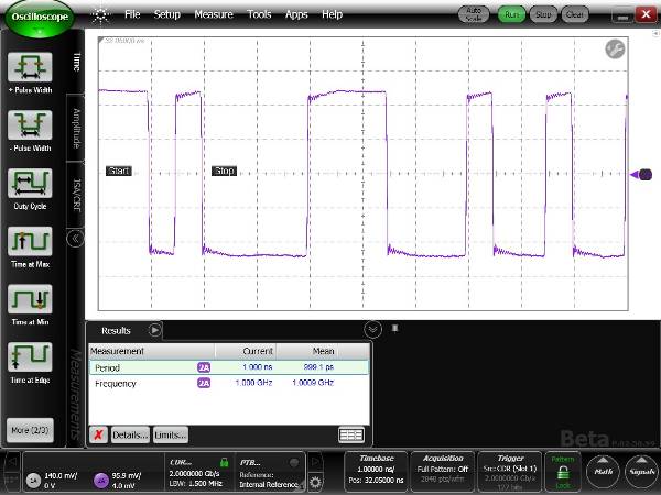
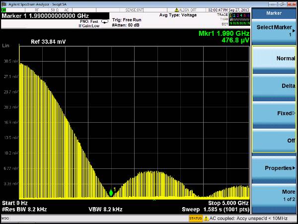 Figures 1A, B, C, D, E, F. Time domain and frequency domain measurements of a 1 GHz sine wave, a 1 GHz square wave, and a 2 Gb/s data flow.
It is also possible to determine the time-domain response of a signal when its frequency components are known. That is, the frequency spectrum of a signal can be used to determine the amplitude-versus-time waveform. This is achieved using the inverse Fourier transform. This applies to all the examples in Figure 1. If the frequency spectrum is known (instead of the time-domain waveform), it is possible to determine the time-domain waveform. Although Figure 1 does not show it, phase information is needed for accurate reconstruction.
When observing digital data on an oscilloscope, one might expect a series of nearly rectangular pulses to represent logic ones and the absence of a pulse to represent logic zeros. The result can be surprising when observing a high-speed digital signal. Logic ones are not so rectangular, and logic zeros may not even be flat lines at a level of 0. Instead, signal edges may exhibit distinct slopes that consume a large portion of the pulse duration or bit period. After a signal transitions from a “0” to a “1” level, it may overshoot and oscillate until it settles at a “final” level. See Figure 2.
 Basic filter theory can explain some of the factors that cause these less-than-ideal data waveforms. When designing a filter, the primary goal is usually to accept a specific frequency range while rejecting a certain range. In light of the previous explanation of the relationship between a signal's frequency content and its time-domain characteristics, it should be clear that passing a waveform through a filter will likely alter its shape. Whenever the frequency spectrum of a signal is altered, its time-domain performance is also altered. Recall the spectrum of the 1 GHz square wave in Figure 1D. What would happen if the signal were transmitted through a low-pass filter that accepted signals below 2 GHz and suppressed frequencies above 2 GHz? The only remaining spectral element would be the 1 GHz tone. The square wave becomes a sine wave. What would happen if the filter accepted frequencies below 4 GHz and rejected frequencies above 4 GHz? The signal would consist of a 1 GHz tone and a 3 GHz tone. The signal would not be a 1 GHz sine wave, but it also wouldn't be the original 1 GHz square wave.
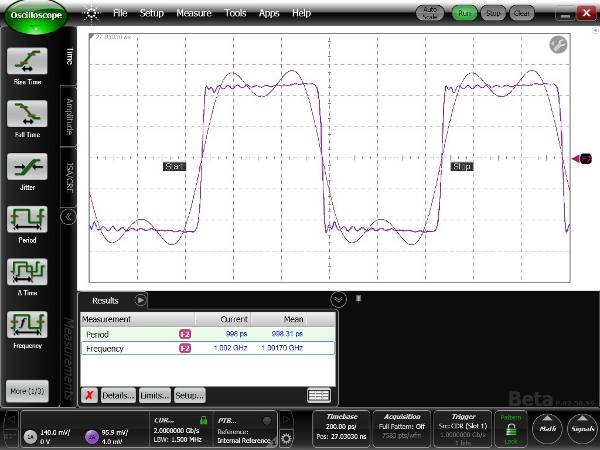 Figure 3 shows the effect of passing the square wave through the low-pass filter. Notice that the rise and fall times of the edges have slowed down. There are also some peaks and dips at the tops and bottoms of the pulses. In fact, the signal looks very much like a fast sine wave (the 3 GHz tone) superimposed on a slower wave (the 1 GHz tone). The filter is doing what is expected of it.
The examples above are quite simple. Real filter designs will not produce these results. Several aspects must be taken into account:
1) Will all frequencies subjected to the filter experience the same propagation delay? If not, how will this affect the waveform in the time domain?
2) Will all signal spectra in the passband experience the same level of attenuation? Some filter designs exhibit ripple (variable attenuation) in the passband, while others exhibit maximization (a small amplification region) before the roll-off. How will this affect the waveform in the time domain?
3) Recall that if the signal spectrum is altered, whether by attenuation, amplification, or by changing the phase relationship between the signal's spectral elements, the waveform will change. Is waveform distortion acceptable?
When designing a filter, it's important to know whether time-domain or frequency-domain characteristics are the priority. Some filters offer excellent frequency suppression at the cost of waveform distortion.
We consider a digital communication system to be functioning correctly when the receiver is able to correctly interpret ones as ones and zeros as zeros. Errors are known as bit errors. The performance of a system is usually described as the bit error rate (BER), that is, how many bits are received incorrectly compared to the total number of bits received. Typical values are on the order of one error per trillion bits transmitted. A low BER is usually achieved when there is a large separation between the level of logical ones and logical zeros, as well as when logical decisions are made "far removed in time" from the transitions of a logical zero to a logical one (or vice versa). The "decision point" is usually located in the middle of the bit (relative to time), halfway between the level of logical ones and logical zeros. If the signal deviates from the ideal and approaches the decision point, the probability of a bad decision increases. Therefore, when bit shapes deviate from ideal "rectangular" waveforms, the bit error rate (BER) can be compromised. In high-speed digital communication networks, waveform distortion is usually due to the alteration of the signal spectrum as it passes through the system. The filter concepts we have just discussed can be applied to high-speed digital communication systems.
One place where it's easy to find a source of waveform distortion is the communication channel. The channel can be any medium that carries the signal from the transmitter to the receiver, such as a copper trace on a PC circuit board, a metallic cable, or a length of fiber optic cable. Most channels exhibit some form of low-pass filter characteristic. There are various mechanisms that attenuate signals with very high frequencies as they propagate along a signal. In PC circuit board traces or metallic cables, this can be attributed to the fact that dielectric materials exhibit higher losses at high frequencies than at low frequencies. High-frequency signals tend to travel along the outer regions of conductors rather than through the entire cross-section of the cable. The effective conductivity is reduced, and attenuation increases. Attenuation of the high-frequency spectrum of a digital signal can have a similar effect to that observed when a square wave is passed through a low-pass filter. The rising and falling edges are slowed down. In the case of an optical fiber, high-frequency losses can occur when the light carrying the digital information travels along different path lengths, since there can be several simultaneous propagation modes (paths) along the fiber. Therefore, the digital information, which propagates as light pulses, will arrive at the receiver time-dispersed. These time-dispersed light pulses have characteristics similar to an electrical pulse that has passed through a low-pass filter. The speed at the edges is reduced, and the pulse shapes change. Again, as the quality of the pulses degrades, the probability of bit errors increases.
The most accurate way to characterize an electrical channel's ability to carry high-frequency signals is to use an instrument called a network analyzer. The network analyzer injects a sine wave into the channel and measures the sine wave exiting at the other end. The ratio of the output to the input indicates the loss that occurs along the cable. By sweeping the sine wave over a wide frequency range, the cable's attenuation characteristic can be determined within that frequency range.
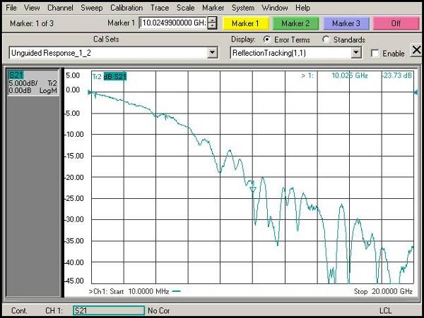 Figure 4 shows a measurement taken with a network analyzer of a signal path along a 25 cm section of a common PC board. Note that at low frequencies, there is hardly any attenuation. However, as the signal frequency increases, so does the attenuation. What does this indicate about the possibilities of using this channel in a high-speed digital communication system? Based on filter theory, the cable's frequency response is somewhat similar to a low-pass filter. Low frequencies pass through almost unchanged, while high frequencies are attenuated. The transmitted bits will be altered as they pass through the channel. What alteration will they undergo? Several approaches can be taken to this end. The cable's frequency response can be mathematically transformed to the time domain using the Fourier transform. The result will be the channel's impulse response. This can be indicative of how a very narrow pulse can be dispersed over time and reduced in amplitude. The ideal pulse signal has a time width of zero. In the frequency domain, this implies an infinite bandwidth. As the ideal pulse passes through the channel, the high-frequency content is eliminated. Again, in the time domain, when the signal leaves the channel, the effect of the high-frequency loss is pulse dispersion. The rise and fall times slow down. How will this affect the quality of communications? Recall that if there isn't a wide separation between the logic one and logic zero levels, the receiver at the end of the channel is more likely to make a mistake when trying to determine the bit level. What effect does pulse dispersion have over time? If the dispersion is severe, the energy of one bit can penetrate the slot allocated to adjacent bits. This phenomenon is known as intersymbol interference (ISI) and is another potential source of receiver error.
At this point, it might seem sensible to forgo the network analyzer and simply inject a real digital communications signal to directly observe the bit quality as it exits the channel using a high-speed oscilloscope. This is a fairly common approach. However, it is standard practice to specify a communications system based on its individual components, such as the transmitter, the channel, and the receiver. This is because the components of a communications system can come from different vendors. Each component must be specified separately. Measuring the frequency response with a network analyzer allows this channel data to be obtained.
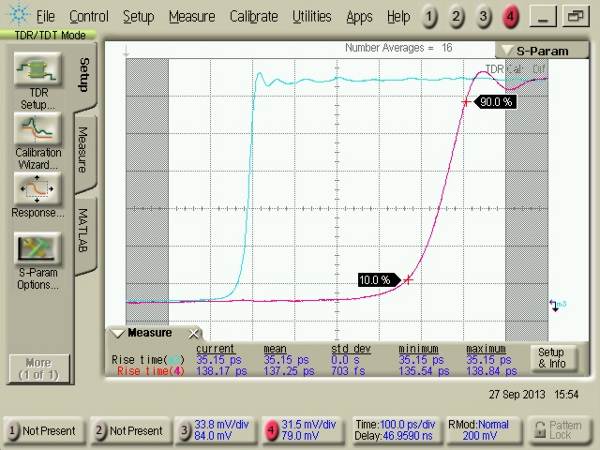
A different but related technique for characterizing a channel involves injecting a very fast step pulse into the channel and observing the pulse at the output using a wide-bandwidth oscilloscope. Comparing the output and input indicates how a channel will degrade digital bits. This technique is known as time-domain transmission, or TDT. Figure 5 shows the TDT response of the channel previously measured with the network analyzer in Figure 4. The input signal is represented by the blue trace. The step, after passing through the PC board, is shown by the red trace. (The real-time delay between input and output is reduced to facilitate comparison of edge rate changes.) This is not the channel's impulse response, but rather its step response. However, similar results can be observed. If the channel were ideal, the output step would be identical to the input step, but with a time delay due to the length of the channel path. However, just as with impulse response, attenuation of the channel's high frequencies slows the speed of the edges. Why? Because the channel has attenuated the high-frequency components of the signal needed to achieve a fast edge.
 The DTT response can be transformed to the frequency domain to display the channel's frequency response. This capability can be integrated into the instrument so that it can provide results similar to those obtained with a network analyzer. Consequently, both the network analyzer and the DTT oscilloscope can offer results in both the time and frequency domains through "native" measurements and transformed results.
The microwave engineer knows that if energy propagates along a transmission line or channel, it's very difficult for the receiver to absorb the entire signal. If the energy isn't absorbed, it has to go somewhere. In most cases, the residual signal is reflected back along the transmission line. This presents two problems. With less signal available in the receiver's decision circuit, the receiver is more likely to make mistakes and degrade the BER (Beat Rate). The second problem is that the reflected energy may return to the transmitter, and if the transmitter can't absorb the reflected signal (its design might not allow it), the signal can be reflected back to the receiver. In that case, the receiver will see two signals, which often conflict. The main signal can be degraded if it's a logic zero and a "phantom" logic one is added to it. Similarly, a logic one with a "phantom" logic zero added to it will be degraded from the ideal signal. In both cases, the separation between ones and zeros will be reduced and the probability of error at the receiver will increase.
This leads to another measurement technique from the microwave world that is becoming increasingly important in digital communications. It is crucial to be able to determine how a signal travels from the transmitter to the receiver through the channel and whether any signal is reflected back from the receiver. A reflection will occur whenever there is a change in the impedance of the signal path. If a transmission line has a characteristic impedance of 50 Ω and the receiver has an impedance of 60 Ω, approximately 9% of the voltage reaching the receiver will be reflected. Reflections can also occur along the channel. Changes in the channel width, caused by holes and connections, dielectric changes, or anything else that could alter the impedance, will result in a signal reflection.
Again, the microwave engineer used a network analyzer to characterize the reflection performance. To perform this measurement, a signal is injected into the test device, such as a cable or integrated circuit, and a directional coupler is used to extract and observe the signals traveling in the opposite direction. The magnitude of the reflected signal is compared to that of the injected signal. The result is called "return loss," and by sweeping the injected signal across a range of frequencies, the return loss can be determined with respect to frequency. Typically, as frequencies increase, it becomes more difficult to control the impedance, and reflections increase.
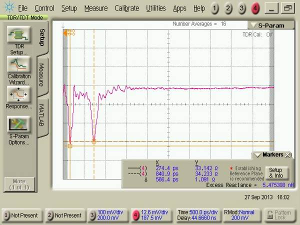
A similar measurement exists in the time domain. It is performed using a wideband oscilloscope and is called a time-domain reflectometer, or TDR. The instrument is essentially identical to the TDT described earlier. However, instead of measuring the pulse of the input signal entering the device and exiting the opposite end, the reflected signals are measured at the same port as the input signal. While the network analyzer displays reflections with respect to frequency, the TDR displays reflections with respect to time. If the propagation speed is known, the TDR operates similarly to radar. By knowing when the reflections (echoes) return to the oscilloscope, the position of the reflection can be precisely determined. The magnitude of any reflection is directly proportional to the impedance. Therefore, the TDR can display impedance with respect to position. Figure 6 shows the screen of a TDR of a 50 Ω transmission line where the impedance drops to 33 Ω, returns to 55 Ω, drops to 33 Ω and returns to 55 Ω.
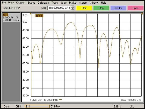
 It is interesting to compare the return loss measurement from the network analyzer with the impedance measurement from the TDR, especially if there are multiple locations where reflections occur. For the TDR, the impedance profile shows each location where the impedance has changed. Where the TDR trace slopes sharply upward, it indicates a location where the impedance has increased. Where it slopes downward, the impedance has decreased. What does the same device look like when measured with the network analyzer? Remember that what is seen is the reflection with respect to frequency. It provides no direct indication of where the reflections occur or whether there is more than one location. Regardless of whether there is one or more locations where reflections occur, the total reflected energy is shown with respect to frequency. An interesting phenomenon can occur if there are two or more impedance discontinuities that are larger than all the others. If two reflections occur, there will be two signals returning to the instrument. Since the signal from the more distant reflection will have traveled a greater distance than the signal from the closer reflection, there will be a phase shift between the first and second reflected signals. The two reflected signals will combine in phase, out of phase by 180 degrees, or somewhere between +/- 180 degrees. The phase relationship depends on the distance between the reflection locations, the propagation speed, and the signal frequency. Because the test signal frequency sweep is usually performed over a wide range, perhaps from 50 MHz to 20 GHz, the two reflected signals are likely to move in and out of phase with each other as the frequency increases. When the two reflected signals are completely out of phase, the total signal will be small (zero, if the two signals are of the same magnitude). If the signals are in phase, the total will be at its maximum. The resulting return loss displayed will vary from maximum to minimum with respect to frequency. Refer to Figure 7. Although the frequency domain signal displayed by the network analyzer cannot directly indicate the presence of multiple reflections, the pattern of systematic maxima and minima in the frequency domain is a common indicator that there are at least two reflections that dominate the overall response.
Figure 7. Screen of a network analyzer showing a transmission line with several locations where reflections occur.
 The vertical axis of the network analyzer is in decibels. In the worst-case scenario, the reflected signal power is 5 dB lower than the transmitted signal, or about 32% of the transmitted signal. The reflected voltage, however, is actually more than 50% higher than the original transmitted signal. This occurs when the signals from the two reflection locations combine in phase. Maintaining impedance is essential for achieving low BER digital communications. In cases where the two reflections combine out of phase, the total reflected signal power is only 30 dB (0.1%) lower than the original transmitted signal. The reflected voltage is 3% of the original. The Fourier transform allows the network analyzer to display the time-domain response in a manner similar to the TDR, and allows the TDR to display the frequency-domain response in a manner similar to the network analyzer.
The phenomenon where the edges of a bit stream do not occur at the expected point in time, but are either ahead or behind, is called “jitter.” As data transmission speeds increase, one of the main problems is ensuring that the receiver does not attempt to make its logical decision while the incoming signal is in the process of changing state. If a decision is made near a signal edge, it will likely increase the bit error rate (BER). Therefore, jitter is a source of BER degradation. What causes jitter? It is due to several mechanisms, for which some knowledge from the world of microwave engineering can be helpful. The rate at which the transmitter sends bits is usually determined by a reference clock. If that clock does not operate at a precise frequency, the transmitted data will be sent at a variable rate. While the digital engineer calls this phenomenon “jitter,” the microwave engineer might call it “phase modulation” or “frequency modulation,” and in this case, it is an unwanted modulation. Instinctively, the microwave engineer will examine the clock in the frequency domain. We previously stated that if the clock emitted an ideal sine wave, a single tone would be observed in the frequency domain. If the clock emitted a square wave, the fundamental tone and its odd harmonic would be present. What would happen if the clock emitted a sine wave with a slightly varying frequency? This is actually quite common. No oscillator is capable of producing a pure tone. There will always be some noise in the internal electronics, and this noise will cause a random fluctuation in the oscillator's frequency. This random fluctuation is observed as a dispersion of the spectrum, centered on the expected frequency. The microwave engineer will call this "phase noise." The rate at which the phase (frequency) changes incorporates a random component.
The digital engineer, accustomed to viewing signals on an oscilloscope, will see edges that are randomly misaligned in time. Instead of calling it "phase noise," they will call it "random jitter." These are two ways of describing the same thing, one from the time domain perspective and the other from the frequency domain perspective. Jitter can also occur systematically. The ISI phenomenon discussed earlier is also a jitter mechanism. Recall that ISI scatters the pulses. If the pulse edges are shifted outward in time from their ideal positions, causing energy to penetrate adjacent bits, we have a jitter mechanism. Jitter can also be periodic. For example, if the transmitter clock has a poorly regulated switching power supply, the switching speed can modulate the frequency. In the time domain, this is called "periodic jitter," while in the frequency domain, it is called "frequency modulation." This phenomenon is difficult to observe directly in the time domain. The effect is likely to spread over thousands or even millions of bits. In the frequency domain, however, this effect is readily apparent. When a signal has undergone frequency modulation, it is easy to observe tones or sidebands above and below the clock tone frequency, with an offset caused by the switching (modulating) signal frequency.
The ability to examine high-speed signals in both the time and frequency domains provides valuable insights into the causes of good or poor performance. Each perspective has its advantages and disadvantages. As data transmission speeds increase, all engineers working with high-speed digital communication systems can benefit from becoming comfortable working in both domains.
By Greg LeCheminant, Agilent Technologies, Inc.