Part 1 described the objectives of interlacing, analyzed the errors that create interlacing artifacts, and presented the range of 40 GSPS analog-to-digital converter (ADC) options using the AD9084. Part 2 presented a direct quadrature sampling option, along with a quadrature correction mechanism in detail. Part 3 presents methods for providing temporal interlacing options.
Figure 1 shows a visual representation of the integrated digital signal processing (DSP) described in Part 1. The clock layout includes provisions for internally inverting the clocks of adjacent ADC channels within the device. The simplest temporal interlacing option is to offload all the data from two channels at the full sampling rate. Unfortunately, this option requires merging the data from two channels within the FPGA or ASIC at the maximum rate before processing. The power consumption and overhead of this option make it less desirable on its own. An alternative temporal interleaving option is one that takes advantage of data filtering within the integrated DSP, such as the quadrature sampling option.

Figure 1. Half of a section of the MxFE receive path, showing two ADCs and an integrated DSP.
The concern for full data rate power creates the need for an option that temporarily interleaves adjacent ADCs, uses the integrated DSP, and downloads data at reduced rates by leveraging digital downconversion (DDC). A method for resolving the ADC's Nyquist limits by leveraging phase information was described below. A unique value demonstrated in these concepts is the option to trade the number of channels for the sampling rate without increasing digital data rates, while still utilizing the programmable integrated DSP capabilities.
Time-Interleaved Segments
Imagine reducing the ADC data to even and odd data samples. Each data stream has half the sampling frequency and contains one sample every two samples shifted. This is what happens when ADC segments are interleaved. Each segment has half the frequency and contains one sample every two samples. The traditional approach is to merge this data at the full sampling frequency. An alternative approach is to use the phase information between the two segments, allowing the Nyquist regions to be resolved without increasing the digital data rates. Figure 2 introduces the concept of interleaved segments visualized in the frequency domain.
For example, let's look at a 2× time-interleaved ADC:
![]()
The sub-ADCs provide the even and odd samples.![]()
![]()
If we interpret the sub-ADC signals in the frequency domain, we can relate them to the desired full speed signal using equations 4 and 5.

Each sub-ADC signal consists of two aliasing signals originating from opposite Nyquist regions. The aliasing polarity differs for even and odd samples. We can exploit this fact to separate the first and second Nyquist regions in post-processing.

Figure 2. Interpretation of intercalated cuts in the frequency domain.
Time interleaving followed by FIR filters.
Working with phase information, a method can be created to solve a Nyquist signal with a first or second cutoff frequency. Figure 3 illustrates one approach to the solution. Recognize that the time delay is

Figure 3. Phase difference between intercalated cuts.
At the ADC output, there is a time delay difference between the two half-period clock segments. This results in a linear phase versus frequency. If a half-sample fractional delay filter is then applied to the output of an ADC channel, the phase is compensated in the first Nyquist plot, but in the second Nyquist plot, there is a phase shift between the interleaved segments. This is the property that should be exploited with the ADC's integrated DSP: a linear phase versus frequency. Therefore, at the ADC output, there is a linear phase versus the input frequency, where the slope is based on the half-period cutoff time delay. The phase difference of both the fundamental and image frequencies is shown in the lower half of Figure 3 compared to the input frequency.
At the ADC output, although we see the phase versus frequency slope, there is not enough information to work with. If we add a half-sample fractional delay to one of the ADC segments, an important property emerges. The result is that the ADC outputs are in phase if the input frequency is at the first Nyquist region and have a 180° phase difference if the signal is at the second Nyquist region. This property allows for a method of summing the signals and creating a Nyquist region cancellation method.
This summation method is useful when the signal of interest is not close to fS/2. For signals that cross the fS/2 boundary, an alternative approach is needed. If a Hilbert transform or a 90° phase shift is added to the fractional digital filter, then the phase delta is in quadrature at the filter outputs. The resulting quadrature also has a phase inversion between I and Q at fS/2 and can be used as quadrature inputs for a complex DDC, making this option analogous to the quadrature sampling option described in Part 2. This can be seen in Figure 4.
Image Correction for Time Interleaving
The previous section discussed various ways in which the outputs of two time-interleaved ADCs can be combined to achieve a 2× full-speed signal, assuming both ADCs are perfectly matched. However, in practice, there will be a gain, phase, and delay mismatch between the ADCs and the branches of the power divider above. As with the quadrature sampling technique, the discrepancy between the ADC paths can be corrected by using a semi-complex filter structure at the ADC output or, alternatively, by summing the outputs of the full complex filters of a pair of DDC channels.
As seen in Figure 5, the time interleaving system can be modeled as an ideal power divider feeding two analog signal paths with different transfer functions, where H0(ω) represents the transfer function of the path capturing the even samples, and H1(ω) represents the transfer function of the path capturing the odd samples. The even and odd signal paths will be referred to as path 0 and path 1.
Figure 4 shows two time-interleaving options that take advantage of the built-in filters. On the left, if a half-sample delay is added to one of the interleaving sections, the signals at the second Nyquist will be in phase and the signals at the second Nyquist will be out of phase. On the right, if a Hilbert transform is included in the FIR coefficients, the result is that the signals are in quadrature at the FIR output with a phase shift at the Nyquist boundaries, similar to quadrature sampling described in Part 2.

Figure 5. A time-interleaving model.
Like QEC, time-interleaving correction is a relative form of equalization. For example, in Figure 6, path 0 can be considered ideal, and path 1 can be equated to path 0. Therefore, the response of path 1 can be modeled as the combination of (a) a nominal delay of 1/2 sample, (b) the common response of path 0, and (c) a mismatch or delta response of path 1 relative to path 0.

Figure 6. A relative time interleaving model in terms of a nominal 1/2 sample delay H0,5 (ω) and a mismatch response HΔ (ω).
Using simple trigonometric identities, the output of path 1 can be decomposed into a sum that includes lagged cosine terms.
![]()

In the absence of mismatch between path 0 and path 1 (i.e., HΔ(ω) = 1), the ideal outputs of the quadrature sampling setup can be defined as:
![]()

Figure 7 shows the result of stimulating this relative time-interleaving model with a sinusoidal input x(t) = cos(ω0 t). The nominal delay of 1/2 sample H0,5(ω) and the mismatch response HΔ(ω) = AΔ(ω) e(jθΔ(ω)) modify the amplitude and phase of the 1-path signal, as shown.

Figure 7. Stimulation of the time-interleaving model with a sinusoidal input.
Therefore, for a sinusoidal or other narrowband signal centered at frequency ω0, the actual outputs can be written in terms of the ideal outputs. The time-interleaving setup can be considered a 2 × 2 linear system that generates a time-interleaving error. Correction of the time-interleaving error is achieved by inverting this 2 × 2 linear system to recover the ideal outputs x0(t) and x1(t), as shown in Figure 8. Note that, for the single-tone case described in this example, the error-correction solution shown in Figure 8 is one of many possible solutions, where the solutions vary by adjusting one filter relative to the other. The error-correction solution becomes unique when attempting to simultaneously correct signals in multiple Nyquist zones, but that unique solution is beyond the scope of this article.
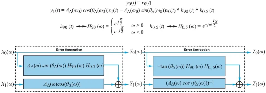
Figure 8. Relative time interleaving model showing both error generation and error correction through a semi-complex filter structure.
The crossover filter extending from path 0 to path 1 must implement a half-sample delay (H0.5(ω)) and a 90° phase shift (H90(ω)).
This time-interleaving error generation model has similarities to the quadrature sampling error generation model, but there is a significant difference. With a single-tone stimulus, quadrature sampling error can be modeled and corrected using single-tap real-value filters. In other words, the correction only requires a gain correction on each of the two real-value filters. However, time-interleaving correction requires a phase correction and therefore requires a multi-tap crossover filter extending from path 0 to path 1.
With the given topology, the outputs z0[n] and z1[n] represent the even and odd samples, respectively, of a 2× interleaved signal sampled at twice the rate. The intertwined output z[n] is constructed as follows:

However, as described in previous sections, the 1/2-sample delay combined with a Hilbert transform can optionally be used to transform z0[n] and z1[n] into a quadrature representation. Figure 9 shows the time-interleaving correction cascade using filters G0(ω) and G1(ω), and the quadrature transformation using Gq(ω), resulting in quadrature outputs z[n] = zi[n] + jzq[n].

Figure 9. Combination of time-interleaving correction, to correct the analog mismatch between path 0 and path 1, with a Hilbert transform to convert it into a quadrature signal representation.
The cascaded filter stages can be merged into a single semi-complex filter structure by including the quadrature transform in the first stage.

Now, with a corrected quadrature output signal, the analysis provided in previous sections can be applied to defer the correction of the ADC output, using the programmable filter (PFILT), to the DDC output, using the complex filter (CFIR).
Figure 10 shows measurements comparing time interlacing with quadrature interlacing when using PFILT or CFIR for their respective error correction. The results show that the errors are approximately equal in magnitude for both time interlacing and quadrature interlacing, and that CFIR offers better performance in both cases.

Figure 10. Image rejection measured by comparing temporal and quadrature interlacing.
Note that the errors are approximately the same and that, in both cases, CFIR correction has improved performance because CFIR operates at decimated speed and the filter taps have a longer effective period.
As described in Part 2, the errors after correction with the PFILT are limited by frequency ripple caused by long transmission lines and impedance mismatch of the RF dividers to the two ADC channels. The PFILT response can approach results similar to those of the CFIR response after correcting the aforementioned problems.
Comparison of Interleaving Options
Multiple interleaving options have been described. A comparison of these options is warranted below. The measurements in Figure 10 show that image rejection performance is virtually the same for quadrature interleaving as for time interleaving, so the decision of which is the best option comes down to other practical application considerations.
Full-Speed Offload vs. Integrated DSP:
In cases where a full 40 GSPS of data is desired, this is possible and can be achieved with the latest MxFE solutions. The practical limitation is absorbing the data increase and then calibrating and reformulating a 40 GSPS data stream before processing. In many cases, it is very convenient to continue monitoring a full 20 GHz Nyquist bandwidth, but using the integrated DSP to reduce the overhead of the digital backend. Options using the integrated DSP have been the focus of most descriptions; however, full-speed data offload remains a realistic option if desired.
Time Interleaving vs. Quadrature Interleaving:
Quadrature interleaving has two advantages:
• Use of the integrated complex-mode FFT
• The input to the quadrature hybrid can be considered as a balanced amplifier. ADC reflections will be passed to the termination port, providing better broadband impedance matching.

The main drawback of quadrature sampling is the limited frequency range of commercially available quadrature hybrids. Commercial components support a range of 2 GHz to 18 GHz, which is historically a wide bandwidth. If even greater bandwidth is desired, resistive power dividers can be used to extend the frequency range to lower frequencies.
PFILT vs. CFIR Correction:
Although both PFILT and CFIR in the AD9084 support time-interleaving correction, each has its advantages and disadvantages. PFILT operates at the ADC's full sampling rate, allowing for the correction of wide bandwidths with a single set of filter coefficients and enabling full use of the built-in DSP functionality. However, CFIR supports longer impulse responses, which directly translates to better performance in this application. Table 1 provides a summary of the advantages and disadvantages.
Conclusion:
This three-part series has described practical methods for enabling first-time Nyquist sampling across 20 GHz using commercially available ADCs. Part 1 introduced the objectives and provided an overview of the options. Part 2 described direct quadrature sampling in detail, along with its shortcomings and necessary corrections. Part 3 concluded with time-interleaving options and a comparison of the available choices. Throughout the series, the technical background for presenting the results obtained, in addition to the final measurements, has been provided.
Considerable effort has been devoted to maintaining dynamic range and noise performance while increasing sampling frequencies. The AD9084 20 GSPS ADCs offer best-in-class performance with input bandwidths up to 18 GHz. The performance of these ADCs has been maintained, while also being increased to 40 GSPS, and user-selectable options have been provided based on application objectives.
Future
work will focus primarily on software and firmware updates that enable optimized integration of interleaving options into final systems. Modifications to the evaluation board will be incorporated to optimize the RF dividers and ADCs.
Acknowledgments
The authors wish to express their gratitude to the design teams. The combination of the ADC's sampling frequencies, input bandwidth, and integrated DSP laid the foundation for developing the concepts discussed. We also want to thank the ADC designers and Analog Devices for their long history, which has paved the way through decades of design work and culminated in the first 20 GHz high dynamic range Nyquist sampling.
References
Ali, Ahmed. High-Speed Data Converters. IET, August 2016.
Kester, Walt. The Data Conversion Handbook. Analog Devices, Inc., 200.
Manganaro, Gabriele. Advanced Data Converters. Cambridge University Press, 2012.
About the Authors:
Ian Beavers is a field applications engineer and customer lab manager for the Aerospace and Defense Systems team at Analog Devices, based in Durham, North Carolina. He has been with the company since 1999. Ian has over 25 years of experience in the semiconductor industry. He holds a Bachelor of Science in Electrical Engineering from North Carolina State University and an MBA from the University of North Carolina at Greensboro.
Peter Delos is a technical lead for the Aerospace and Defense Group at Analog Devices in Greensboro, North Carolina. He earned his Bachelor of Science in Electrical Engineering from Virginia Tech in 1990 and his MBA from NJIT in 2004. Peter has over 30 years of experience in the industry. He has spent most of his career designing advanced analog and RF systems at the architecture, PCB, and IC levels. Currently, he focuses on miniaturizing receiver designs, waveform generators, and high-performance synthesizers for phased-array applications.
Brian Reggiannini is a senior principal systems design engineer. He has designed, implemented, and supported system-level calibrations for several generations of Analog Devices wireless transceiver products. His technical interests include signal processing, machine learning, embedded systems, and systems involving digitally assisted analog components. Brian earned his Sc.B., Sc.M., and Ph.D. degrees from Brown University in 2007, 2009, and 2012, respectively.
Connor Bryant is a systems applications engineer at Analog Devices, working in the aerospace and defense business unit in Durham, North Carolina. He joined ADI in 2023. He currently focuses on the design and analysis of RF mixed-signal chains. He obtained his Bachelor of Science in Electrical Engineering from North Carolina State University in 2022 and his Master of Science in Electrical Engineering from the same university in 2023.