 During the photolithography process, wafers are coated with a photoresistant film and then exposed to masking patterns to protect one area of the wafer while work is being done on another. Etching and ion implantation are performed to create electrical circuits. These processes are then repeated until the circuit is finally completed.
At the end of the process, several additional layers are applied for insulation and sealing before the chip passes final part testing. During these processes, the wafers must be continuously transported and kept isolated from external influences. Therefore, the semiconductor manufacturing process requires a large number of subsystems.
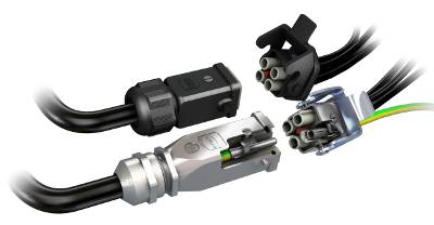
HARTING connectors have long been used for the main power supply of various subsystems. The product range used in semiconductor production already covers power ranges from 40 to 200 A. Motors, handling systems, vacuum pumps, and heaters can now be designed as connectorized units with a HARTING solution using Han® Q 3/0 and Han® Q 4/0 connectors. Their simple locking systems offer significant time and safety advantages in this application area. Crimp termination technology also ensures a high degree of quality and flexibility during assembly. The compact design of the Han® 3 A base offers additional advantages when space is limited. The Han® series connectors (Han® Q 3/0 and Han® Q 4/0) increase the reliability of power transmissions and operational safety, a critical requirement in the semiconductor industry. Furthermore, manufacturing and maintenance costs are reduced.